
 Search
 en
en English
 日本語
日本語 русский
 Español
 Deutsch
 中文简体
中文简体Content
- 1 What Is a Glass Wafer?
- 2 Core Advantages of Precision Glass Wafers
- 3 Standard Glass Wafer Specifications
- 4 Available Glass Materials
- 5 Applications in the Electronics Industry
- 6 Applications in Optics
- 7 Manufacturing Process for High-Precision Glass Wafers
- 8 Why Manufacturing Capability Matters
- 9 Advantages Compared with General-Purpose Suppliers
- 10 How to Specify a Custom Glass Wafer
- 11 Typical Customer Benefits
- 12 Quality Risks and How They Are Controlled
- 13 Q&A: Frequently Asked Questions About Glass Wafers
- 13.1 What industries use glass wafers?
- 13.2 What standard wafer diameters are available?
- 13.3 Can the wafer thickness be customized?
- 13.4 What does a surface quality specification of 20/10 mean?
- 13.5 Why are flatness and warpage important?
- 13.6 Which glass material is best for high-temperature applications?
- 13.7 Can glass wafers be used for optical components?
- 13.8 Can wafers include locating features?
- 13.9 What information is needed for a quotation?
- 13.10 How should glass wafers be handled?
- 13.11 What makes a specialist manufacturer different from a general glass supplier?
- 14 Conclusion
- 15 References
- 16 Product: Glass Wafer
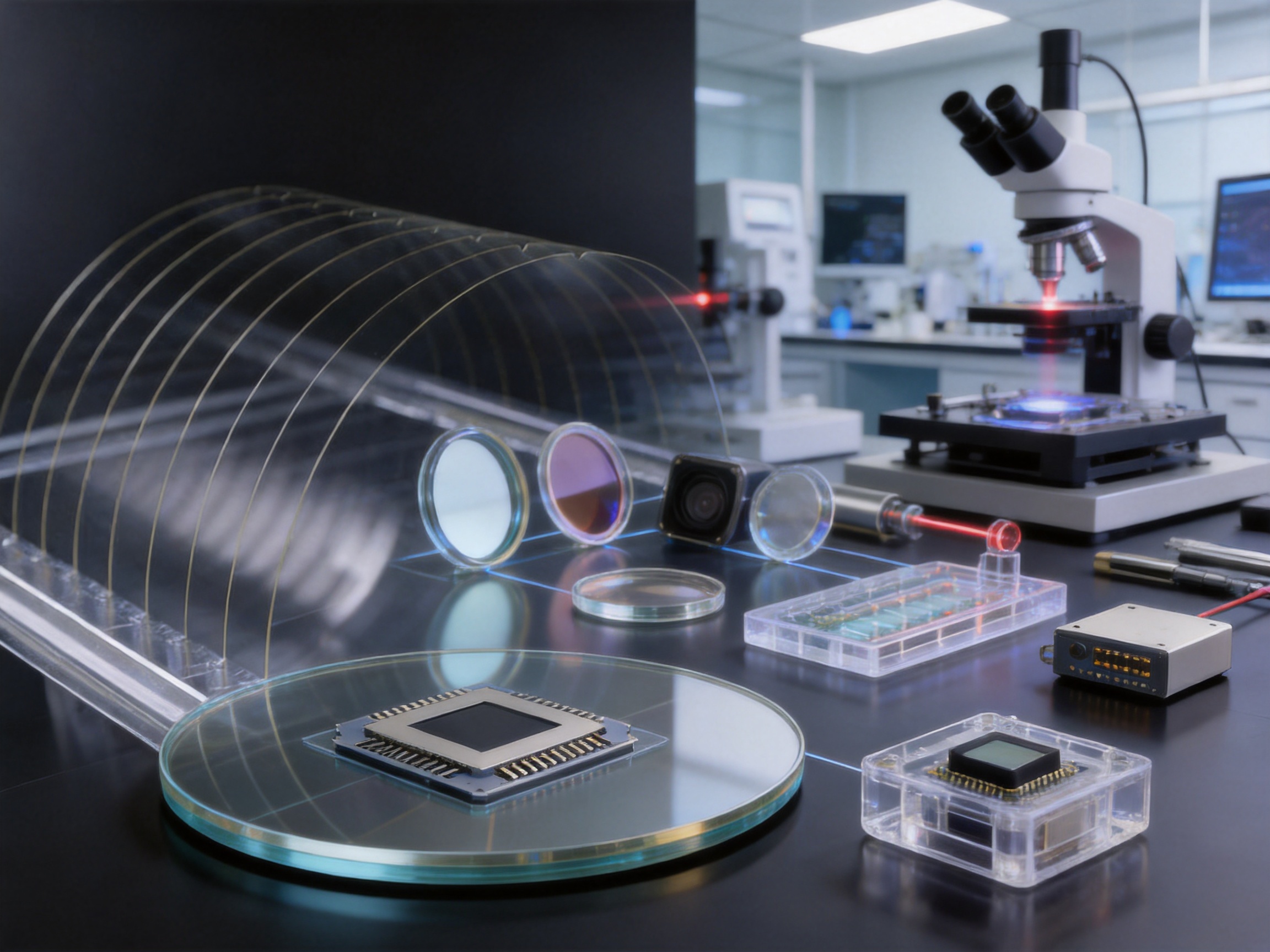
Glass wafers are essential enabling components in many advanced technologies. They provide a stable, transparent, chemically resistant, and dimensionally controlled platform for semiconductor processing, microelectromechanical systems, optical assemblies, sensors, communication devices, and scientific instruments. As electronic and optical products become smaller, more integrated, and more demanding, the quality of the wafer substrate directly influences manufacturing yield, device reliability, alignment accuracy, and long-term performance.
High-precision glass wafers are not simply thin discs of glass. They are engineered substrates whose diameter, thickness, flatness, surface roughness, warpage, edge geometry, and optical properties must be controlled within narrow tolerances. The right material and manufacturing process are also critical. A wafer used for a MEMS package may require excellent thermal stability and chemical durability, while a wafer intended for an optical application may require high transmission, low scattering, and excellent homogeneity.
Changzhou Haolilai Photo-Electricity Scientific and Technical Co., Ltd. specializes in the long-term production of precision glass wafers for industrial, electronic, optical, and scientific applications. The company supports standard wafer sizes as well as customized dimensions, materials, thicknesses, edge forms, and locating features. Its manufacturing capabilities are supported by a large production site, an experienced technical team, certified quality systems, and long-term experience in precision optical component production.
This article explains the characteristics, applications, materials, specifications, manufacturing considerations, and selection advantages of high-precision glass wafers. It also describes how a professional manufacturer can support demanding projects that require stable quality, repeatable tolerances, and dependable customization.
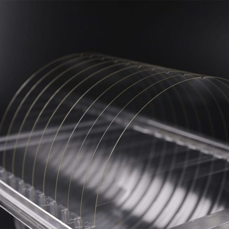
Glass Wafer
What Is a Glass Wafer?
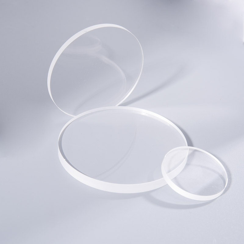
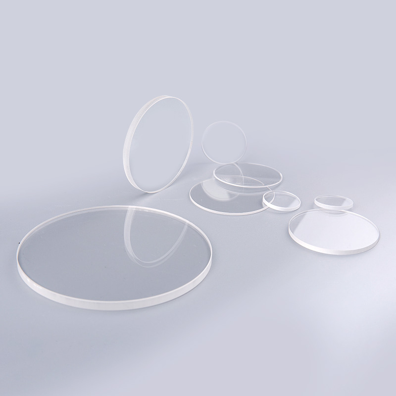
A glass wafer is a thin, flat, typically circular substrate manufactured from specialty glass. It may be used as a structural support, an optical element, a processing carrier, a device substrate, or a packaging component. Depending on the intended application, the wafer can be supplied as a plain round disc, a disc with a locating edge, or a disc with one or more locating angles.
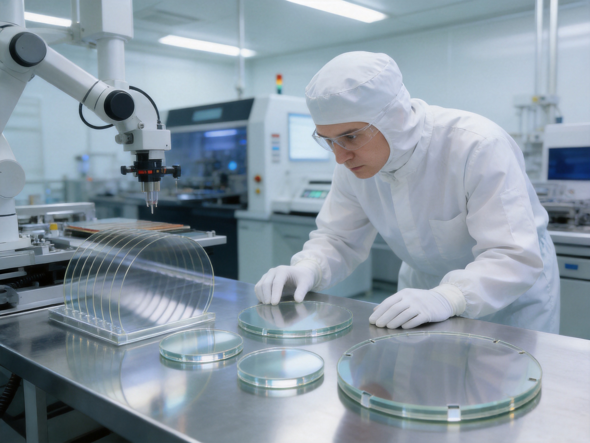
Unlike ordinary glass sheets, precision glass wafers are manufactured and finished to meet controlled geometric and surface requirements. The wafer may be ground, polished, cleaned, inspected, and packaged under carefully controlled conditions. The final product must maintain its specified dimensions while avoiding defects that could interfere with deposition, bonding, lithography, etching, coating, or optical transmission.
Glass is especially valuable as a wafer material because it combines several useful properties in one substrate. It offers good transparency, low fluorescence intensity, a low expansion coefficient in suitable grades, strong resistance to thermal shock, positive chemical stability, scratch resistance, and low alkali content. These properties make glass suitable for processes and environments in which ordinary materials may deform, contaminate, discolor, or lose dimensional accuracy.
The wafer’s performance depends on the specific glass composition. Sodalime glass may be suitable for cost-sensitive or general-purpose applications, while Pyrex, Borofloat, borosilicate glass, D263T, Corning E-XG, and BK7 may be selected for better thermal stability, improved optical performance, or specialized processing requirements. A professional supplier can help match the substrate material to the temperature range, chemistry, transmission band, bonding method, and mechanical demands of the final device.
Core Advantages of Precision Glass Wafers
High Optical Transparency
Glass provides a transparent platform for applications involving visible light, ultraviolet-adjacent wavelengths, sensors, imaging, and optical measurement. Its transmission performance can be tailored by selecting an appropriate glass type and controlling the quality of the finished surfaces. This makes glass wafers useful for optical filters, lens components, mirrors, camera modules, laser systems, and scientific instruments.
Optical transparency is also important when a device must be inspected through the substrate. In some microelectronic, sensor, and MEMS designs, the ability to transmit light through the wafer supports alignment, monitoring, imaging, or optical activation. A clean, uniform glass surface helps prevent unwanted scattering and visual distortion.
Low Fluorescence Intensity
Low fluorescence intensity is valuable in imaging, analytical, biomedical, and scientific applications. Unwanted fluorescence from a substrate can interfere with signal detection, reduce measurement accuracy, and increase background noise. By using suitable glass materials and controlling surface cleanliness, a glass wafer can provide a more stable platform for sensitive optical measurements.
Low and Controlled Thermal Expansion
Thermal expansion affects alignment, bonding, coating, lithography, and the mechanical stability of assembled devices. Glass materials with a low or controlled coefficient of thermal expansion can help reduce dimensional changes when temperature varies. This is particularly beneficial for semiconductor packaging, sensor substrates, optical benches, and components that must remain accurately aligned during operation.
Thermal compatibility is also important when a glass wafer is joined to silicon, metal, ceramic, or another glass. Selecting materials with compatible expansion behavior helps reduce stress at interfaces and lowers the risk of cracking, delamination, or warpage during thermal cycling.
Strong Thermal Shock Resistance
Precision glass wafers may encounter rapid temperature changes during processing or service. Thermal shock resistance helps the substrate tolerate heating and cooling transitions without sudden fracture. Borosilicate-based materials are frequently considered for applications involving elevated temperatures, laboratory equipment, chemical processing, and repeated thermal cycling.
Thermal shock resistance does not eliminate the need for proper process control. Heating and cooling rates, edge quality, wafer thickness, clamping methods, and surface defects all influence performance. A carefully finished wafer with smooth edges and controlled geometry is better positioned to withstand demanding handling and process conditions.
Chemical Stability
Many semiconductor, MEMS, and optical processes involve cleaning agents, etchants, solvents, photoresist materials, coatings, or bonding chemicals. Glass is valued for its chemical stability and inert surface characteristics. The appropriate glass grade can provide resistance to many process environments while maintaining its transparency and dimensional integrity.
Material selection must always be based on the actual chemical exposure. Different glass compositions have different resistance levels to acids, bases, solvents, moisture, and high-temperature processes. A technical manufacturer can assist customers in selecting the correct substrate rather than treating all glass wafers as interchangeable.
Scratch Resistance and Surface Stability
Surface quality is critical for wafer processing. Scratches, pits, particles, stains, and polishing marks can interfere with thin-film deposition, photolithography, bonding, coating, and optical performance. Properly polished glass wafers provide a stable surface with low roughness and controlled cosmetic quality.
The specified surface quality of 20/10 reflects a high level of control for precision applications. Combined with a typical roughness of Ra ≤ 1 nm, this surface condition supports demanding optical and electronic processes where microscopic irregularities can influence yield or performance.
Low Alkali Content Options
Low alkali glass is useful for applications in which mobile ions could affect electrical performance, film adhesion, device stability, or process cleanliness. In electronic and semiconductor environments, substrate composition must be considered carefully because trace elements can migrate under heat or electric fields.
Glass wafers manufactured from suitable low-alkali materials can help provide a cleaner, more stable base for device fabrication. Material selection should be determined by the required electrical, thermal, optical, and chemical characteristics of the finished product.
Standard Glass Wafer Specifications
The manufacturer offers common wafer diameters from 4 inches to 12 inches, together with custom dimensions for specialized projects. The minimum stated product capability is a thickness of at least 0.1 mm and an outer dimension of at least 2 inches, subject to the detailed requirements of the project.
| Specification | 4 Inch | 5 Inch | 6 Inch | 8 Inch | 12 Inch |
|---|---|---|---|---|---|
| Nominal diameter | 100 ± 0.1 mm | 125 ± 0.1 mm | 150 ± 0.1 mm | 200 ± 0.1 mm | 300 ± 0.1 mm |
| Typical thickness | 500 ± 5 µm or customized | 625 ± 5 µm or customized | 675 ± 5 µm or customized | 725 ± 5 µm or customized | 900 ± 5 µm or customized |
| Surface roughness | Ra ≤ 1 nm | Ra ≤ 1 nm | Ra ≤ 1 nm | Ra ≤ 1 nm | Ra ≤ 1 nm |
| Warpage | ≤ 10 µm | ≤ 10 µm | ≤ 10 µm | ≤ 10 µm | ≤ 10 µm |
| Flatness | ≤ 3 µm | ≤ 3 µm | ≤ 3 µm | ≤ 3 µm | ≤ 3 µm |
| Surface quality | 20/10 | 20/10 | 20/10 | 20/10 | 20/10 |
The dimensions shown above represent standard configurations. Actual production requirements may vary according to the material, wafer diameter, thickness, edge profile, inspection method, and application. Custom tolerances should be reviewed before production so that the manufacturing and inspection plan can be aligned with the customer’s technical drawings.
Diameter Control
Diameter tolerance influences equipment compatibility, wafer handling, mask alignment, fixturing, packaging, and the usable area of the substrate. A tolerance of ±0.1 mm supports repeatable positioning in many industrial applications. For projects with unusual dimensions or tighter requirements, customized diameter control may be discussed with the technical team.
Thickness Control
Thickness affects mechanical strength, thermal behavior, optical path length, weight, and compatibility with processing equipment. Standard thicknesses are available for the most common wafer diameters, while customized thicknesses can be considered for thin substrates, optical assemblies, specialty packaging, and experimental devices.
Thickness uniformity is as important as nominal thickness. A wafer that is the correct thickness at one point but varies excessively across its surface may create problems during deposition, bonding, lithography, or optical alignment. Precision grinding and polishing are therefore essential stages in achieving consistent wafer geometry.
Flatness and Warpage
Flatness describes the deviation of the wafer surface from a defined reference plane, while warpage describes the overall bending or bowing of the substrate. The listed flatness value of ≤ 3 µm and warpage value of ≤ 10 µm support applications requiring stable contact with chucks, masks, fixtures, bonding tools, or deposition equipment.
Improved flatness can help reduce nonuniform contact, improve film thickness consistency, and support more accurate pattern transfer. Low warpage is particularly important for larger wafers because the risk of deformation generally increases as the diameter grows.
Edge Geometry
Glass wafers can be supplied with inverted edges in configurations such as 45-degree edges, SEMI-style edges, or C-shaped edges. Edge geometry affects handling safety, fracture resistance, equipment compatibility, and the available usable area near the perimeter.
A properly finished edge reduces sharp corners and minimizes the likelihood of chipping during transport or automated handling. For semiconductor and MEMS applications, a locating edge or locating angle can also establish a repeatable orientation for processing and inspection.
Available Glass Materials
Sodalime Glass
Sodalime glass is a widely used material that can offer a practical balance between availability, transparency, manufacturability, and cost. It may be appropriate for general-purpose substrates, education and research, selected optical components, and applications without severe thermal or chemical requirements.
Because sodalime glass has different thermal and chemical characteristics from borosilicate or optical crown glass, it should be selected only after reviewing the operating environment and process conditions.
Pyrex and Borosilicate Glass
Pyrex and borosilicate materials are widely recognized for useful thermal performance, chemical durability, and resistance to thermal shock. They are often considered for laboratory equipment, MEMS structures, semiconductor packaging, microfluidic components, and applications involving repeated heating and cooling.
Borosilicate glass can also be useful when a substrate must maintain dimensional stability over a broad temperature range. The exact composition and grade should be confirmed for every project because thermal expansion, transmission, and chemical behavior vary among products.
Borofloat
Borofloat is a borosilicate-type material commonly used where good thermal properties, chemical resistance, and optical transparency are important. It can serve as a substrate for microfabrication, optical assemblies, and precision industrial components.
Borosilicate D263T
D263T is a specialty borosilicate glass frequently considered for thin, precise, and optically demanding applications. Its controlled properties can make it useful for sensor windows, microelectronic structures, thin glass substrates, and precision optical components.
Corning E-XG
Corning E-XG is a specialty glass option for applications that require a carefully controlled substrate material. It may be selected for electronic, display-related, sensor, and advanced research applications where surface quality, dimensional stability, and composition are important.
BK7
BK7 is a well-known optical glass used in lenses, prisms, windows, and other precision optical components. BK7 wafers can be considered when optical homogeneity, transmission, and predictable refractive behavior are essential. They may be used in camera systems, laser equipment, scientific instruments, and optical prototypes.
For projects requiring another glass grade, the manufacturer can evaluate custom material sourcing and processing requirements. The correct choice should consider wavelength range, refractive index, thermal expansion, chemical exposure, mechanical loading, surface treatment, and the final assembly process.
Applications in the Electronics Industry
Integrated Circuit Substrates
Glass wafers can serve as stable substrates for integrated circuit-related processing, thin-film deposition, circuit patterning, and experimental semiconductor structures. Their smooth and inert surfaces support the application of conductive, dielectric, semiconductor, and protective layers.
As electronic devices become smaller, process uniformity becomes increasingly important. Variations in flatness, thickness, or surface roughness may affect lithography focus, coating uniformity, etch behavior, and bonding quality. A precision wafer helps provide a repeatable starting point for these operations.
MEMS Fabrication
Microelectromechanical systems combine mechanical structures with electrical or sensing functions. Glass wafers can be used as device substrates, cover plates, bonding partners, or packaging components. Their transparency can allow visual or optical inspection of internal structures, while their chemical and thermal characteristics can support several microfabrication processes.
Glass is also useful in anodic bonding and other wafer-level packaging approaches, provided that the selected glass composition and surface condition are compatible with the bonding process. Low roughness and strong flatness are particularly valuable because bonding quality depends on intimate and uniform contact between mating surfaces.
CMOS and CCD Sensor Packaging
Image sensors and other optoelectronic devices require substrates and covers that maintain optical clarity while protecting delicate active structures. Glass wafers can be processed into cover windows, package substrates, or optical interfaces for CMOS and CCD-related products.
Low fluorescence, good transmission, low defect density, and suitable surface cleanliness are important in imaging applications. The wafer must also meet the dimensional and edge requirements of the packaging equipment used by the customer.
Communication and Data Processing Devices
Optical communication and data-processing systems rely on stable components for transmitting, directing, filtering, and detecting light. Glass substrates can be used in optical modules, photonic structures, sensor packages, and precision alignment assemblies.
In such systems, even a small dimensional deviation may affect coupling efficiency or component alignment. A wafer with controlled thickness, flatness, and optical quality can help improve repeatability during assembly.
Applications in Optics
Optical Windows and Filters
Glass wafers can be used as the base material for optical windows, filters, protective covers, and coated substrates. The substrate can be supplied with a polished surface and later receive an antireflection coating, reflective coating, bandpass coating, conductive coating, or other functional layer.
Surface quality is important because coating defects often originate from contamination, scratches, pits, or polishing irregularities on the substrate. A clean and uniform wafer provides a better foundation for subsequent coating processes.
Lenses, Mirrors, and Prisms
Although a glass wafer is normally flat, it can be used as a starting substrate for manufacturing optical lenses, mirrors, prisms, and other components. Its controlled material properties and high-quality surface allow manufacturers to perform later shaping, coating, or bonding operations.
BK7 and other optical glasses are especially relevant when refractive index, dispersion, transmission, and homogeneity must be controlled. For precision optical systems, the quality of the original glass substrate influences the efficiency and consistency of subsequent processing.
Camera and Imaging Systems
Camera modules, machine vision systems, telescopes, microscopes, and analytical instruments require optical components with low scattering and stable transmission. Precision glass wafers may be used for sensor covers, optical windows, calibration components, and thin substrates that are integrated into compact modules.
As imaging systems become more compact, components must fit within tighter mechanical envelopes. Custom wafer diameters, thicknesses, locating features, and edge profiles can support specialized optical designs that cannot be served by standard catalogue parts.
Laser and Scientific Equipment
Laser systems and scientific instruments often require substrates with good optical homogeneity, stable surfaces, and predictable thermal behavior. Glass wafers can provide a controlled platform for optical coatings, beam-conditioning elements, measurement windows, and experimental photonic structures.
In high-sensitivity instruments, the substrate’s fluorescence, internal quality, surface scattering, and environmental stability may be important selection criteria. A technical review before production helps ensure that the chosen material and surface specification are suitable for the wavelength and operating conditions.
Manufacturing Process for High-Precision Glass Wafers
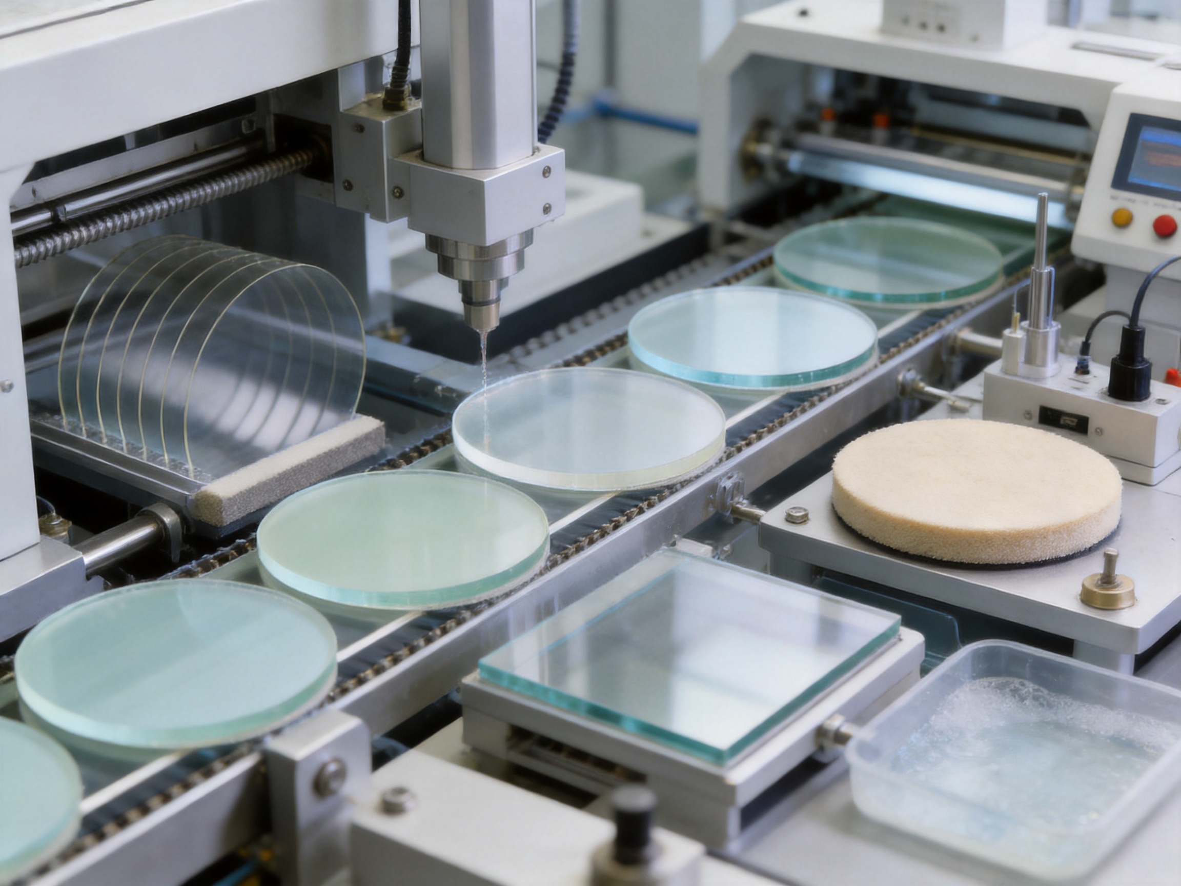
The manufacturing of precision glass wafers involves a series of controlled operations. The exact process varies according to material, diameter, thickness, edge configuration, and final application, but a professional production route generally includes material preparation, blank formation, dimensional processing, edge finishing, precision grinding, polishing, cleaning, inspection, and packaging.
Material Review and Blank Preparation
Production begins with the selection and review of the specified glass material. The manufacturer considers the required diameter, thickness, thermal properties, optical requirements, chemical environment, and processing compatibility. Glass blanks are then prepared in a form suitable for precision machining.
Material consistency is important because variations in composition or internal quality can influence transmission, stress, thermal expansion, and polishing behavior. Using an appropriate material at the beginning of production helps prevent performance problems later in the process.
Precision Cutting and Shaping
The glass blank is cut or shaped to approach the required wafer diameter. This stage must control edge chipping, dimensional deviation, and internal stress. Oversize material may be retained for later grinding and finishing, allowing the final dimensions to be reached gradually.
For custom shapes or locating features, the production plan may include special cutting and machining steps. Round wafers with locating edges or locating angles require accurate orientation and repeatable feature placement.
Edge Processing
Edge processing is a critical safety and reliability step. Sharp or damaged edges can create handling hazards and may act as initiation points for cracks. Edge inversion, beveling, or C-shaped finishing can improve handling behavior and reduce chipping risk.
The selected edge style should match the customer’s equipment and process standards. Semiconductor-oriented applications may require a specific SEMI-style profile, while research or optical applications may use a 45-degree or C-shaped edge.
Grinding and Thickness Control
Grinding establishes the basic thickness and improves parallelism between the two wafer surfaces. Controlled abrasive processing removes saw marks, surface damage, and irregularities left from the initial shaping stage.
Careful control of grinding pressure, abrasive conditions, fixturing, and cooling helps limit subsurface damage and deformation. Excessive mechanical stress at this stage could make later polishing more difficult or increase the possibility of warpage.
Precision Polishing
Polishing refines the surface to achieve the required roughness, flatness, and optical quality. The objective is not merely to create a visually bright surface. Precision polishing must produce a consistent surface condition across the entire wafer while preserving the required geometry.
The listed surface roughness of Ra ≤ 1 nm and surface quality of 20/10 indicate a high-quality finish suitable for demanding optical and electronic applications. Polishing parameters must be adapted to the glass composition because different materials respond differently to abrasives, polishing pads, pressure, and chemical polishing agents.
Cleaning and Contamination Control
After polishing, wafers must be cleaned to remove abrasive residue, particles, oils, and other contaminants. Cleaning is especially important for semiconductor, MEMS, sensor, and optical coating applications. A contamination-controlled surface supports better adhesion, more stable deposition, and improved bonding performance.
Packaging materials and handling procedures are also selected to protect the finished wafer. Gloves, protective films, separators, and suitable containers can help prevent fingerprints, scratches, and particulate contamination before the product reaches the customer.
Inspection and Quality Verification
Inspection verifies that the finished wafer meets its drawing and purchase specifications. Depending on the project, inspection may include diameter measurement, thickness measurement, thickness uniformity, flatness, warpage, surface roughness, visual defect inspection, edge inspection, and optical examination.
Documented inspection is particularly important for repeated orders. It allows the manufacturer and customer to compare batches, identify trends, and maintain consistent product performance over time. Quality systems certified to ISO9001:2015 provide a structured framework for process control and continual improvement.
Why Manufacturing Capability Matters
Choosing a glass wafer supplier requires more than comparing nominal prices. The supplier’s ability to maintain consistent tolerances, process different materials, manage custom requirements, and support technical communication can have a direct effect on the total cost of the customer’s project.
A wafer that is inexpensive but inconsistent may create additional expenses through rejected batches, process interruptions, rework, broken components, or poor device yield. By contrast, a manufacturer with established precision-processing capabilities can help reduce uncertainty during development and volume production.
Experience in Precision Optical Components
Changzhou Haolilai Photo-Electricity Scientific and Technical Co., Ltd. was founded in 1998 and specializes in precision optical components. Its product focus includes laser optics, automotive optics, semiconductor optics, and consumer optics. This broad experience is relevant to glass wafer production because many wafer requirements overlap with the needs of optical windows, lenses, mirrors, prisms, and coated substrates.
Optical manufacturing experience supports attention to surface quality, transmission, homogeneity, cleanliness, edge condition, and geometric precision. These factors are important not only in optical components but also in semiconductor and MEMS substrates.
Large Production Site and Technical Team
The company covers approximately 35,000 square meters and employs more than 300 people. Its scale supports dedicated production, engineering, inspection, and customer-service functions. A larger technical organization can be beneficial when a project requires material evaluation, process development, drawing review, prototype production, and transition to repeat orders.
The company has also established the Jiangsu Precision Optical Lens Engineering Technology Center and the Jiangsu Enterprise Technology Research Center. These technical resources support product development and process improvement for demanding optical and electronic applications.
Quality and Environmental Systems
The company has obtained ISO9001:2015 and ISO14001:2015 certifications, as well as IATF16949 certification. ISO9001:2015 provides a framework for quality management, process documentation, customer requirements, corrective action, and continual improvement. ISO14001:2015 addresses environmental management. IATF16949 is associated with quality management requirements in the automotive industry.
These certifications are particularly relevant for customers that require formal supplier qualification, traceability, controlled documentation, and stable production procedures. They also demonstrate that manufacturing is organized around repeatable systems rather than relying solely on individual operator experience.
Support for International Customers
The company exports to more than 20 countries and holds more than 30 certificates and patents. International experience can help simplify technical communication, documentation, packaging coordination, and production scheduling for overseas customers.
For custom glass wafers, the supplier can review drawings, material requirements, surface specifications, edge profiles, and packaging expectations before quotation. This helps ensure that the final product is evaluated according to the customer’s actual application rather than a generic wafer description.
Advantages Compared with General-Purpose Suppliers
General glass suppliers may offer discs or sheets, but they may not provide the same level of wafer-specific control. High-precision glass wafers require close attention to thickness uniformity, flatness, warpage, edge design, surface quality, and application compatibility.
One important advantage is the ability to supply both standard and customized sizes. Standard 4-inch, 5-inch, 6-inch, 8-inch, and 12-inch wafers can simplify equipment integration, while custom diameters and thicknesses support research programs, specialty sensors, optical prototypes, and low-volume industrial products.
A second advantage is material flexibility. The availability of Sodalime, Pyrex, Borofloat, borosilicate D263T, Corning E-XG, BK7, and other materials allows customers to select a substrate based on thermal, optical, chemical, or electrical requirements.
A third advantage is the combination of optical-component expertise and structured quality management. Customers can work with a manufacturer familiar with precision surfaces and optical tolerances while also benefiting from process systems intended to support repeatable production.
A fourth advantage is the ability to address edge and orientation requirements. Locating edges, locating angles, 45-degree inverted edges, SEMI-style edges, and C-shaped edges can be incorporated into the design when required. These details may appear small, but they can be essential for automated handling and repeatable processing.
How to Specify a Custom Glass Wafer
Define the Application
Begin by identifying whether the wafer will be used for semiconductor processing, MEMS fabrication, optical coating, sensor packaging, imaging, laboratory research, or another purpose. The application determines the importance of thermal expansion, optical transmission, chemical resistance, electrical behavior, and surface cleanliness.
Select the Material
Specify the preferred glass grade if the material is already established. If not, provide the wavelength range, process temperature, chemical exposure, bonding method, and mechanical requirements. A technical manufacturer can then recommend a suitable material or compare several alternatives.
Specify Dimensions and Tolerances
Provide the nominal diameter, diameter tolerance, thickness, thickness tolerance, thickness uniformity, flatness, and warpage requirements. If the wafer must fit a particular tool, include the equipment model or interface dimensions where possible.
Define Surface and Edge Requirements
State the required roughness, surface quality, polish condition, coating condition, and inspection standard. Edge requirements should include the edge profile, bevel dimensions, locating edge or angle, and any limits on chips or cracks.
Confirm Packaging and Documentation
For sensitive applications, specify individual separation, protective films, clean packaging, batch identification, inspection reports, material certificates, and traceability requirements. Proper packaging protects the wafer after it has passed final inspection.
Typical Customer Benefits
Using a well-controlled glass wafer can improve process repeatability by providing a consistent starting surface. This may contribute to more uniform deposition, more predictable bonding, improved lithography behavior, and lower variation between devices.
Glass wafers can also simplify optical integration. Their transparency allows light to pass through the substrate, making them suitable for sensor windows, imaging packages, optical alignment structures, and inspection-friendly devices.
Material flexibility helps customers optimize the balance between cost and performance. A standard material may be appropriate for a general-purpose product, while a specialty optical or borosilicate grade may be justified for a demanding thermal or optical environment.
Customization can reduce the need for secondary machining by delivering the desired diameter, thickness, edge shape, and locating features from the supplier. This may lower handling risk and shorten the customer’s internal production cycle.
Quality Risks and How They Are Controlled
Common quality risks in glass wafer production include chips, cracks, scratches, particles, thickness variation, warpage, excessive roughness, edge damage, and material mismatch. Each risk can affect the customer’s process differently.
Chips and cracks may cause breakage during handling or thermal cycling. Edge processing and careful inspection help reduce this risk. Scratches and pits may lower optical transmission or interfere with coatings and thin-film deposition. Precision polishing and surface inspection address these issues.
Thickness variation can create nonuniform process conditions, while warpage may cause poor contact with a chuck or bonding surface. Controlled grinding, polishing, fixturing, and geometric inspection are needed to maintain the specified wafer profile.
Material mismatch can lead to thermal stress, chemical attack, or optical performance outside the required range. Reviewing the application before production helps prevent this problem. The manufacturer’s experience with multiple glass types is valuable when customers are still evaluating material options.
Q&A: Frequently Asked Questions About Glass Wafers
What industries use glass wafers?
Glass wafers are used in semiconductor manufacturing, MEMS, CMOS and CCD sensor packaging, optical communications, data processing, imaging, laser systems, scientific research, electronic products, and specialty industrial equipment.
What standard wafer diameters are available?
The standard configurations include 4-inch, 5-inch, 6-inch, 8-inch, and 12-inch wafers. Other diameters can be customized according to project requirements. The listed nominal diameters are approximately 100 mm, 125 mm, 150 mm, 200 mm, and 300 mm respectively.
Can the wafer thickness be customized?
Yes. Standard thicknesses are available for each common diameter, and customized thicknesses can be considered. The stated product capability includes thicknesses of at least 0.1 mm, subject to the selected material, diameter, tolerance, and application.
What does a surface quality specification of 20/10 mean?
20/10 is a commonly used optical surface-quality designation describing allowable scratch and dig characteristics. The exact inspection method and acceptance criteria should be confirmed for the project, but the designation indicates a precision optical surface rather than a general-purpose glass finish.
Why are flatness and warpage important?
Flatness and warpage affect contact with processing tools, mask alignment, bonding, coating uniformity, and device assembly. Low deviation helps the wafer remain stable during fabrication and reduces variation across the usable surface.
Which glass material is best for high-temperature applications?
There is no single material that is best for every high-temperature application. Pyrex, Borofloat, and other borosilicate materials are often considered because of their thermal shock resistance and chemical stability. The final choice should be based on the actual temperature range, heating and cooling rate, chemical environment, and mating materials.
Can glass wafers be used for optical components?
Yes. Glass wafers can serve as substrates or starting materials for optical windows, filters, lenses, mirrors, prisms, sensor covers, and laser components. BK7 and other optical glass grades may be selected when refractive index, transmission, dispersion, and homogeneity are important.
Can wafers include locating features?
Yes. Wafers can be supplied as round substrates with locating edges or locating angles. Edge configurations may include 45-degree inverted edges, SEMI-style edges, and C-shaped edges, depending on the application and equipment requirements.
What information is needed for a quotation?
Important information includes material, diameter, thickness, tolerances, surface roughness, flatness, warpage, surface quality, edge geometry, locating features, quantity, inspection requirements, packaging, and intended application. Drawings or samples are helpful for custom projects.
How should glass wafers be handled?
Wafers should be handled with clean gloves or suitable vacuum tools, protected from scratches and particles, and stored in appropriate separators or containers. Customers should avoid placing polished surfaces directly against hard or contaminated surfaces.
What makes a specialist manufacturer different from a general glass supplier?
A specialist manufacturer is equipped to control wafer-specific geometry, polish quality, edge conditions, material selection, inspection, and repeatability. It can also support technical customization and integrate the product into more demanding semiconductor, optical, MEMS, and electronic manufacturing processes.
Conclusion
High-precision glass wafers provide a combination of transparency, low fluorescence, thermal stability, chemical resistance, surface durability, and dimensional control that is difficult to replace with ordinary substrate materials. They support a wide range of advanced applications, from CMOS and CCD sensor packaging to MEMS fabrication, integrated circuit processing, optical coating, laser systems, and scientific research.
The available standard sizes cover common 4-inch through 12-inch wafer formats, while customized diameters, thicknesses, materials, edge profiles, and locating features support specialized designs. Specifications such as Ra ≤ 1 nm roughness, flatness of ≤ 3 µm, warpage of ≤ 10 µm, and 20/10 surface quality are suitable for applications requiring controlled surfaces and reliable geometry.
Changzhou Haolilai Photo-Electricity Scientific and Technical Co., Ltd. combines long-term precision optical manufacturing experience with a broad material range, custom production capability, structured quality systems, and technical resources. Founded in 1998, the company serves customers in multiple international markets and focuses on laser optics, automotive optics, semiconductor optics, consumer optics, and related precision components.
For customers seeking a stable and adaptable glass wafer supplier, the most important considerations are not only nominal dimensions and price. Material suitability, process capability, inspection discipline, edge quality, surface condition, customization support, and production consistency are equally important. A carefully specified and professionally manufactured glass wafer can provide a dependable foundation for higher-yield processing, accurate optical performance, and long-term product reliability.
References
1. ISO 9001:2015, Quality Management Systems—Requirements.
2. ISO 14001:2015, Environmental Management Systems—Requirements with Guidance for Use.
3. IATF 16949, Quality Management System Requirements for Automotive Production and Relevant Service Parts Organizations.
4. Optical glass and precision optical component manufacturing principles, including surface quality, polishing, flatness, and dimensional inspection practices.
5. Semiconductor and MEMS substrate processing principles, including wafer handling, thin-film deposition, bonding, lithography, and surface cleanliness requirements.
6. Technical product specifications for precision glass wafers, including standard diameters, thicknesses, roughness, flatness, warpage, surface quality, edge configurations, and available glass materials.
7. General engineering references on borosilicate glass, optical crown glass, soda-lime glass, thermal expansion, chemical durability, and optical transmission.


 苏公网安备32041102000130号