
 Search
 en
 English
 日本語
 русский
 Español
 Deutsch
 中文简体
Content
- 1 What Is a Quartz Wafer?
- 2 Core Advantages of High-Purity Quartz Wafers
- 3 Available Dimensions and Technical Specifications
- 4 Surface Quality and Dimensional Precision
- 5 Manufacturing Process for Precision Quartz Wafers
- 6 Manufacturing Strengths and Quality Systems
- 7 Advantages Compared with Conventional Glass and Standard Substrates
- 8 Applications of Quartz Wafers
- 9 Customization Options
- 10 How to Select the Correct Quartz Wafer
- 11 Packaging, Handling, and Storage
- 12 Why Work with an Experienced Custom Manufacturer?
- 13 Quality Assurance from Prototype to Production
- 14 Frequently Asked Questions
- 14.1 What are quartz wafers mainly used for?
- 14.2 What standard wafer diameters are available?
- 14.3 Can the thickness be customized?
- 14.4 Are both sides polished?
- 14.5 What surface roughness can be achieved?
- 14.6 What does a 20/10 surface quality mean?
- 14.7 Can the wafer include a locating edge?
- 14.8 Are quartz and sapphire wafers the same?
- 14.9 Which material sources are available?
- 14.10 Can the manufacturer support prototypes?
- 14.11 What information should be included in an inquiry?
- 14.12 How should quartz wafers be handled?
- 14.13 Can quartz wafers be used in ultraviolet systems?
- 14.14 Why is low warpage important?
- 15 Conclusion
- 16 References
- 17 Product: Quartz Wafer
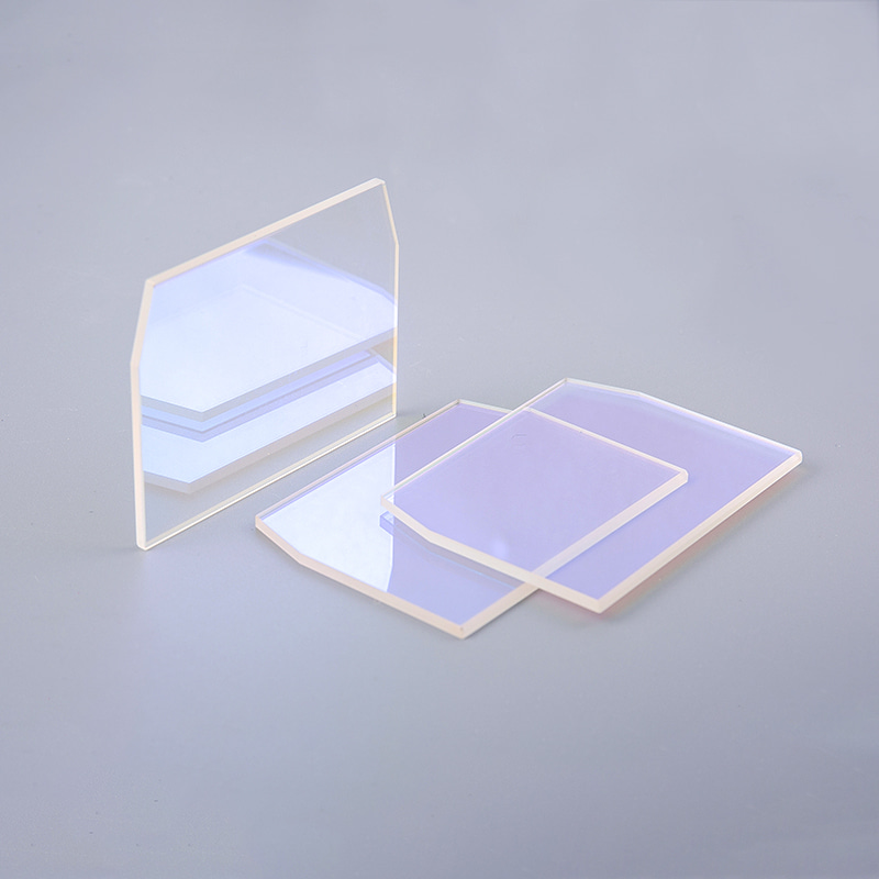
Quartz wafers are precision-engineered substrates designed to combine optical clarity, dimensional stability, mechanical strength, and reliable electrical performance in a single material platform. Their unique balance of properties makes them suitable for demanding applications in photonics, laser systems, spectroscopy, imaging, microelectromechanical systems, planar waveguide devices, and advanced semiconductor manufacturing.
Unlike ordinary glass substrates, high-quality quartz wafers offer exceptionally low thermal expansion, strong transmission across ultraviolet, visible, and near-infrared wavelengths, and low optical absorption and scattering. These characteristics help maintain dimensional accuracy and optical consistency when a component is exposed to temperature changes, intense illumination, vacuum processing, or repeated handling during fabrication.
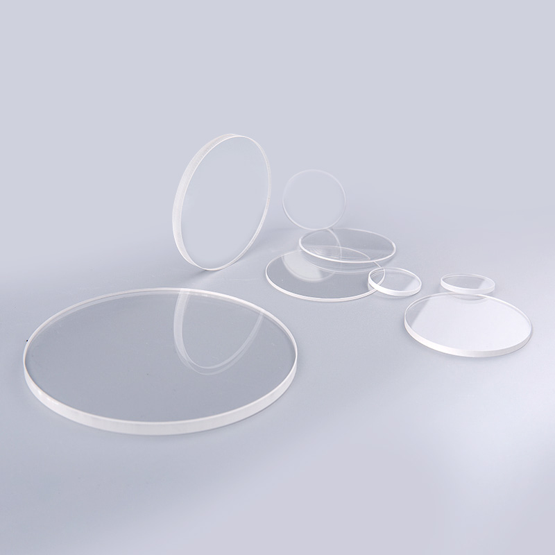
Precision quartz wafers are available in standard diameters from 2 inches to 8 inches, with larger sizes and special geometries available through customization. Typical products can be supplied with double-sided polishing or single-sided polishing, fine surface roughness, controlled warpage, low total thickness deviation, locating edges, and defined edge profiles. Such specifications support the needs of laboratories, equipment manufacturers, optical system integrators, and high-volume industrial users.
Changzhou Haolilai Photo-Electricity Scientific and Technical Co., Ltd. is an experienced Chinese manufacturer of precision optical components and custom wafer products. Since 1998, the company has developed manufacturing capabilities serving laser optics, automotive optics, semiconductor optics, and consumer optics. Its production facilities, technical personnel, quality systems, engineering centers, certifications, and international customer experience provide a strong foundation for producing customized quartz wafer solutions.
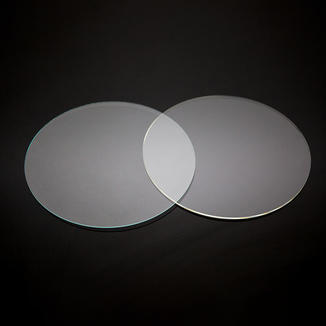
Quartz Wafer
What Is a Quartz Wafer?
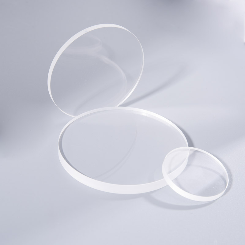
A quartz wafer is a thin, flat, circular substrate manufactured from high-purity quartz or fused silica. It is processed into a controlled diameter and thickness and then finished to meet specified requirements for flatness, surface roughness, parallelism, edge geometry, cleanliness, and optical quality. Depending on the application, a wafer may be used as a standalone optical window, a carrier substrate, a microfabrication base, or a starting material for deposited, etched, bonded, or patterned structures.
Quartz is valued because it remains stable in conditions that can challenge many conventional materials. It has a low coefficient of thermal expansion, which means that its dimensions change only slightly when temperature varies. This is particularly important for lithography, interferometry, spectroscopy, laser beam delivery, and precision alignment systems, where even small dimensional changes can affect performance.
Quartz also has excellent optical transmission over a broad spectral range. High-quality material can transmit ultraviolet, visible, and near-infrared radiation with low absorption. Consequently, quartz wafers can be incorporated into optical windows, photonic devices, laser components, sensor structures, and imaging assemblies. The material is also chemically resistant and electrically insulating, making it suitable for manufacturing environments involving plasma, vacuum, chemicals, elevated temperatures, and high-frequency electrical operation.
The term “quartz wafer” can describe products with different grades, material sources, and surface treatments. The appropriate selection depends on wavelength, operating temperature, processing chemistry, required surface quality, electrical behavior, and the intended fabrication method. For this reason, the wafer should be specified not only by diameter and thickness, but also by material grade, surface finish, edge condition, optical quality, cleanliness, and inspection requirements.
Core Advantages of High-Purity Quartz Wafers
Low Thermal Expansion
One of the most important advantages of quartz is its low thermal expansion coefficient. When temperature changes, a quartz substrate experiences less dimensional movement than many common glass, ceramic, or metal alternatives. This stability helps preserve alignment, feature placement, and optical path length in precision systems.
For semiconductor and MEMS applications, thermal stability can reduce stress during heating and cooling cycles. For optical systems, it helps maintain the designed geometry of lenses, windows, prisms, and waveguide structures. For metrology and laboratory equipment, it can improve repeatability and reduce the need for frequent recalibration.
Broad Optical Transmission
Quartz wafers provide useful transmission in the ultraviolet, visible, and near-infrared ranges. This broad spectral response allows one material to serve different optical systems without requiring multiple substrate types. The material is suitable for laser optics, spectroscopy, imaging, ultraviolet sensors, optical communication components, and scientific instruments.
Low optical absorption is valuable in high-power laser applications because absorbed energy can lead to localized heating, thermal lensing, or coating damage. Low scattering is similarly important when the wafer is used in imaging, detection, interferometry, or beam-shaping systems. Proper polishing and cleaning further improve the practical optical performance of the finished wafer.
High Purity and Chemical Resistance
High-purity quartz minimizes contamination that could interfere with semiconductor processing, thin-film deposition, optical transmission, or microfabrication. Its resistance to many chemicals also supports use in wet processing, cleaning, etching, and laboratory environments.
Material purity must be matched to the application. Semiconductor users may require strict control of metallic impurities, particles, hydroxyl content, and outgassing behavior. Optical users may place greater emphasis on transmission, homogeneity, birefringence, inclusions, and surface quality. A qualified manufacturer can help identify the most appropriate material specification rather than treating every quartz wafer as identical.
Mechanical Strength and Processing Stability
Quartz combines relatively high tensile strength with a stable, rigid structure. Although thin wafers must still be handled carefully, properly manufactured substrates can tolerate demanding processing and repeated use. Their rigidity supports accurate mounting and reduces unwanted deformation during inspection, coating, bonding, and assembly.
Mechanical performance depends on thickness, diameter, edge design, surface condition, internal defects, and handling practices. A rounded or chamfered edge can reduce chipping risk compared with a sharp edge. Controlled edge profiles such as a 45-degree chamfer or C-shaped edge can also improve compatibility with fixtures and automated handling systems.
Electrical Insulation
Quartz is electrically insulating and has useful dielectric properties. This makes it attractive for MEMS devices, high-frequency structures, sensors, semiconductor equipment components, and electrically isolated optical assemblies. Its electrical stability can support applications where the substrate must withstand electric fields without becoming a conductive path.
In device manufacturing, the wafer may be combined with conductive films, piezoelectric layers, semiconductors, or dielectric coatings. The quartz substrate provides a stable base while the deposited or patterned layers perform the active electrical or mechanical function.
Available Dimensions and Technical Specifications
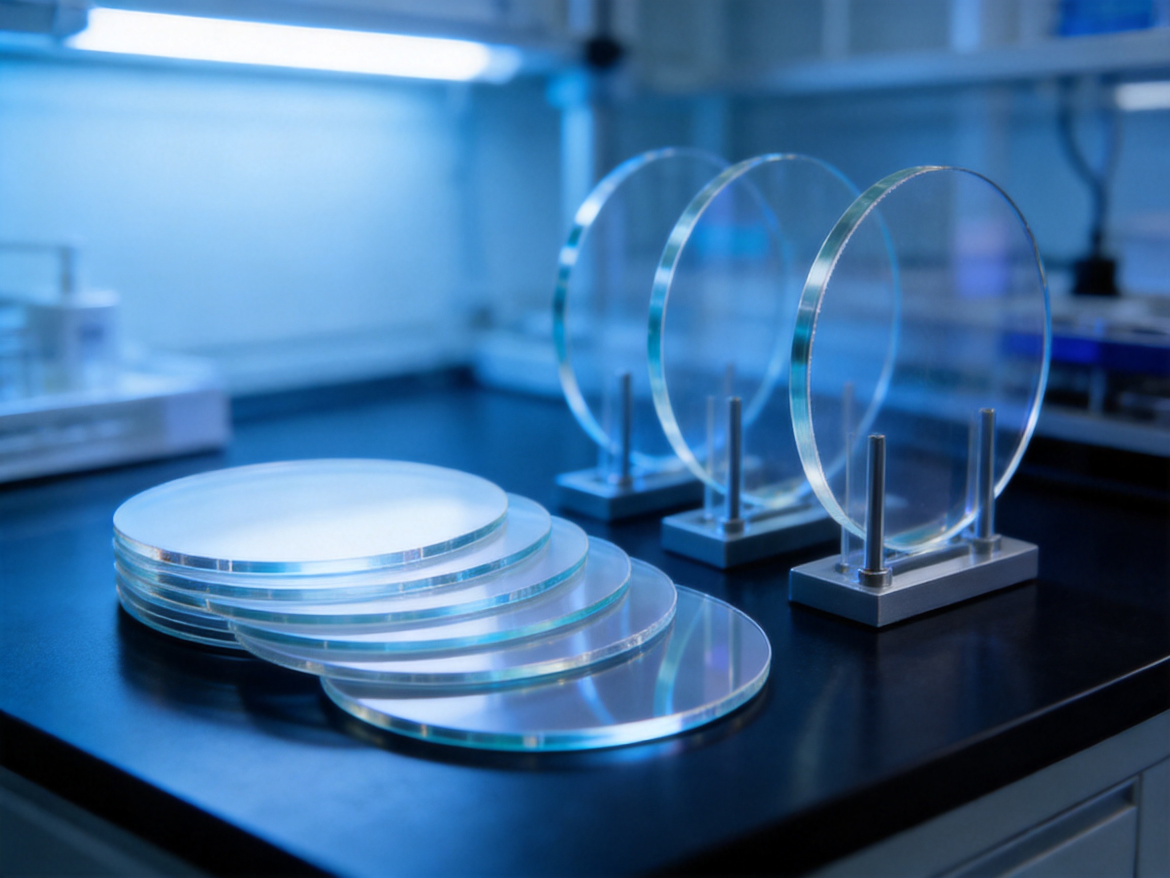
Standard dimensions help customers integrate quartz wafers into existing process tools, fixtures, inspection equipment, and packaging systems. The supplied specifications include common 2-inch, 4-inch, 6-inch, and 8-inch diameters. Other diameters can be manufactured according to drawings, process requirements, or equipment compatibility.
| Specification | 2-Inch Wafer | 4-Inch Wafer | 6-Inch Wafer | 8-Inch Wafer |
|---|---|---|---|---|
| Nominal diameter | 2 inches | 4 inches | 6 inches | 8 inches |
| Diameter tolerance | 50.8 ± 0.1 mm | 100 ± 0.1 mm | 150 ± 0.1 mm | 200 ± 0.1 mm |
| Typical thickness | 430 ± 25 µm or customized | 650 ± 25 µm or customized | 1300 ± 25 µm or customized | 1300 ± 25 µm or customized |
| Surface roughness | Ra ≤ 0.3 nm | Ra ≤ 0.3 nm | Ra ≤ 0.3 nm | Ra ≤ 0.3 nm |
| Warpage | ≤ 10 µm | ≤ 10 µm | ≤ 10 µm | ≤ 10 µm |
| Total thickness deviation | ≤ 3 µm | ≤ 3 µm | ≤ 3 µm | ≤ 3 µm |
| Surface quality | 20/10 | 20/10 | 20/10 | 20/10 |
| Surface options | Double-sided polishing or single-sided polishing | |||
| Shape | Round wafer with locating edge options | |||
| Edge options | 45-degree chamfer or C-shaped edge | |||
The dimensions in the table represent standard reference values. Actual requirements may vary according to the customer’s equipment, process temperature, coating system, handling method, and final assembly. Thicknesses of 0.1 mm and above can be considered for custom designs, subject to diameter, flatness, mechanical strength, and manufacturing feasibility.
For applications involving automated handling, a locating edge can improve orientation control. For manual laboratory use, edge geometry may be selected primarily to improve safety and reduce chipping. For wafer bonding or thin-film deposition, the customer may require a specific combination of thickness uniformity, surface roughness, flatness, and cleanliness.
Surface Quality and Dimensional Precision
Surface quality is a central factor in the performance of a quartz wafer. A wafer used as an optical window must have low scattering and minimal defects. A wafer used for lithography or microfabrication must offer a sufficiently flat and uniform surface for coating, exposure, alignment, and etching. A wafer used for bonding must provide controlled roughness and cleanliness on the bonding surface.
Surface Roughness
The specified roughness of Ra ≤ 0.3 nm represents a highly refined surface condition. Such a surface can reduce microscopic scattering, improve contact uniformity, and support thin-film and bonding processes. Surface roughness may be specified independently for each side because the front and back surfaces can serve different purposes.
Double-sided polishing is useful when both faces must meet controlled optical or dimensional requirements. It can improve parallelism and provide a more uniform substrate for processing. Single-sided polishing may be selected when one surface is the functional face and the reverse side is used for mounting, handling, or mechanical support.
Warpage and Flatness
Warpage describes the departure of the wafer from an ideal flat reference plane. A maximum warpage of 10 µm is suitable for many precision optical and microfabrication applications, although some processes may require tighter limits. Low warpage improves contact with vacuum chucks, masks, bonding fixtures, deposition stages, and inspection platforms.
Flatness must be considered together with thickness variation, edge effects, surface waviness, and local irregularities. A wafer may meet an overall warpage requirement while still exhibiting local features that affect a particular process. Therefore, customers should define whether they need global flatness, local flatness, site flatness, total thickness variation, or a combination of these parameters.
Total Thickness Deviation
Total thickness deviation of ≤ 3 µm provides a controlled basis for device processing, optical mounting, and multi-wafer assembly. Uniform thickness supports consistent exposure focus, predictable etch depth, stable thermal behavior, and repeatable mechanical positioning.
Thickness requirements should be selected according to the wafer diameter and application. Very thin substrates may require special handling, support carriers, or temporary bonding. Larger wafers may need additional attention to stress relief, edge treatment, and polishing parameters to preserve uniformity across the entire surface.
Optical Surface Quality
A 20/10 surface quality designation indicates a high level of control over scratches and digs under the applicable inspection method. This type of finish is appropriate for many precision optical applications where visible surface defects could increase scattering or reduce image quality.
Optical quality requirements should also address inclusions, bubbles, striae, haze, wedge, parallelism, and transmitted wavefront distortion when relevant. These properties are influenced by both the raw material and the processing route. A customer requiring high-performance laser or imaging components should communicate the operating wavelength, beam power, aperture, angle of incidence, and environmental conditions before finalizing the specification.
Manufacturing Process for Precision Quartz Wafers
Producing a high-precision quartz wafer requires coordinated control of material selection, cutting, shaping, grinding, polishing, cleaning, inspection, and packaging. Each stage affects the final optical, mechanical, and dimensional performance of the substrate.
Material Selection and Incoming Inspection
The process begins with selection of suitable high-purity quartz or fused silica material. Material sources may include recognized international suppliers such as Corning, Nikon, Heraeus, or other approved sources, depending on the required grade and availability. Alternative materials can be evaluated for custom projects.
Incoming inspection typically considers material identity, dimensions, visible inclusions, homogeneity, transmission characteristics, and documentation. For semiconductor or scientific applications, additional controls may be required for trace impurities, hydroxyl content, internal stress, and chemical compatibility.
Blank Preparation and Cutting
The selected material is prepared into a wafer blank using precision cutting equipment. Cutting parameters are controlled to reduce chipping, subsurface damage, thermal stress, and dimensional variation. The cutting direction and material orientation may be chosen according to the optical or mechanical requirements of the project.
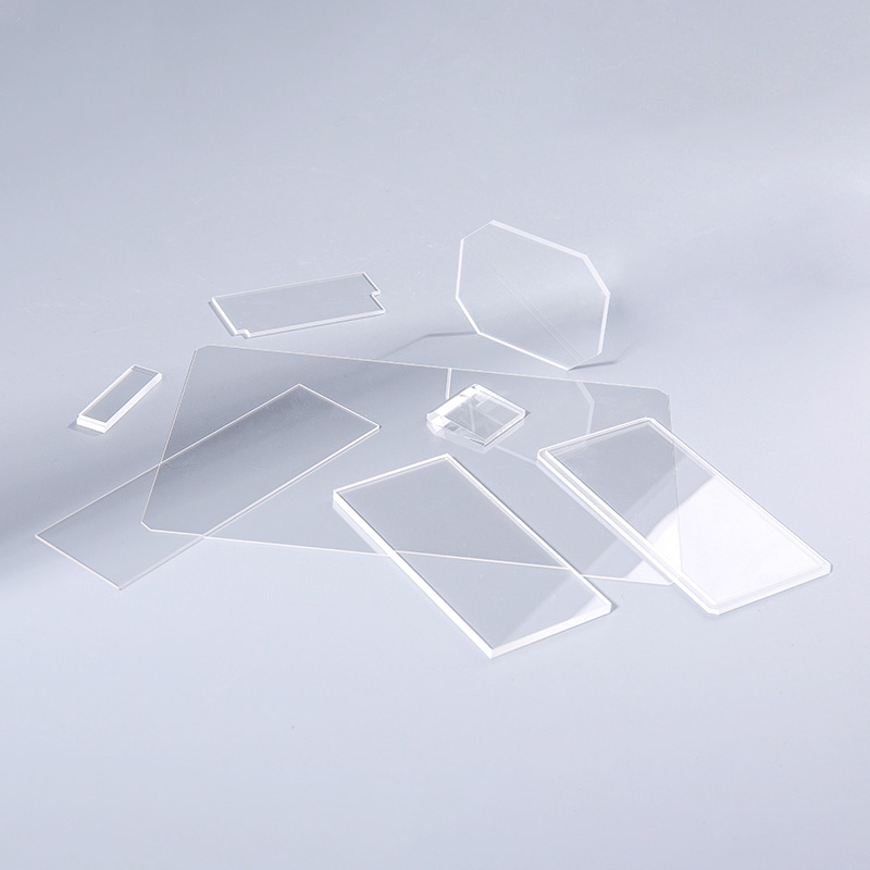
For custom wafers, the blank preparation stage can accommodate special diameters, thicknesses, locating edges, or nonstandard patterns. Early review of the customer’s drawing helps determine whether the product should be manufactured from a standard blank or a specially prepared starting piece.
Edge Shaping
After cutting, the wafer edge is shaped and finished. A defined 45-degree chamfer or C-shaped edge can reduce sharp corners, improve handling safety, and lower the risk of edge damage. The edge profile may also be selected for compatibility with carriers, vacuum chucks, robotic tools, or wafer storage systems.
Edge finishing is more than a cosmetic operation. Small chips or cracks at the perimeter can propagate during thermal cycling or mechanical handling. Proper edge grinding and polishing help protect the wafer and improve its service reliability.
Grinding and Thickness Control
Precision grinding removes cutting damage and brings the wafer close to its target thickness. The grinding process must balance material removal rate with stress control. Excessive mechanical force can produce subsurface damage, while insufficient removal may leave cutting marks or irregular thickness.
Thickness is measured during production to guide subsequent processing. For large wafers or thin substrates, the process may require carefully controlled pressure distribution, tooling conditions, and support methods. The goal is to achieve uniform thickness without introducing excessive residual stress or warpage.
Fine Lapping and Polishing
Lapping and polishing refine the surface condition and improve flatness, parallelism, and optical quality. The process can be configured for one-sided or double-sided polishing. Double-sided polishing is especially beneficial when both surfaces must be controlled or when parallelism is important.
Fine polishing uses progressively smaller abrasive particles and carefully managed process conditions. Slurry selection, pad condition, pressure, rotation, temperature, and cleaning intervals all influence the final roughness and defect level. Process stability is essential because a wafer can lose dimensional accuracy if polishing is not uniform across the full aperture.
Cleaning and Contamination Control
After polishing, wafers are cleaned to remove abrasive residues, particles, organic contamination, and handling marks. Cleaning procedures are selected according to the intended application. Semiconductor and MEMS users may require more stringent particle and ionic contamination controls than general optical users.
Clean handling, appropriate packaging materials, and controlled storage help preserve the surface condition after final inspection. Protective packaging also reduces the risk of scratches, fingerprints, and edge damage during transportation.
Inspection and Final Verification
Final inspection verifies the parameters agreed with the customer. These may include diameter, thickness, thickness deviation, warpage, surface roughness, surface quality, edge profile, locating-edge position, appearance, and cleanliness.
Optical inspection equipment can identify scratches, digs, chips, inclusions, and other defects. Dimensional instruments verify wafer geometry and thickness. Surface measurement systems evaluate roughness, while flatness and warpage equipment confirms the shape of the completed wafer. Inspection records can be supplied when required by the project.
Manufacturing Strengths and Quality Systems
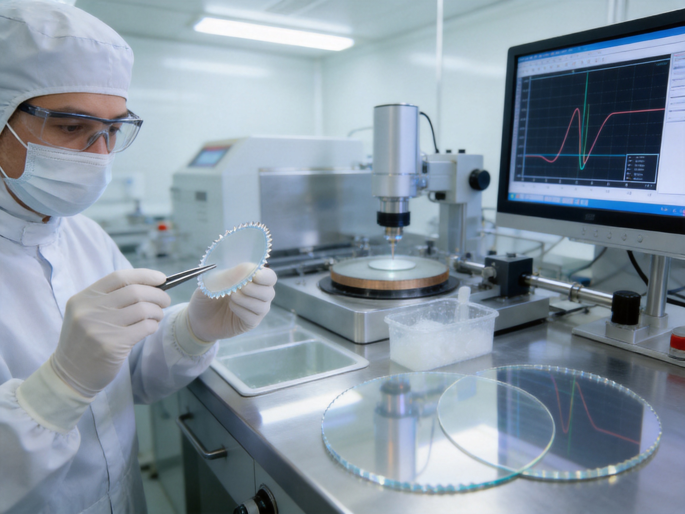
The manufacturer behind these quartz wafer solutions has operated in the precision optical industry since 1998. Its long-term experience provides practical knowledge in optical design support, material selection, precision grinding, polishing, coating-related preparation, inspection, and custom component production.
The company operates on a site of approximately 35,000 square meters and has more than 300 employees. Its production scope includes laser optics, automotive optics, semiconductor optics, and consumer optical components. This diversified experience is valuable because wafer projects often require knowledge that crosses traditional product categories. For example, a semiconductor substrate may require optical-grade polishing, while an optical window may require wafer-like dimensional control.
Quality and environmental management systems include ISO 9001:2015 and ISO 14001:2015 certification. The company also holds IATF 16949 certification, which is particularly relevant to customers in the automotive supply chain. These systems support controlled documentation, process management, traceability, corrective action, supplier control, and continuous improvement.
Technical development is supported by the Jiangsu Precision Optical Lens Engineering Technology Center and the Jiangsu Enterprise Technology Research Center. The company has also obtained invention patents, utility model patents, and recognized high-technology products. These capabilities indicate an engineering-oriented approach rather than a purely catalog-based manufacturing model.
International experience is another important strength. The company exports to more than 20 countries and has accumulated experience communicating specifications, packaging requirements, inspection documentation, and delivery expectations with overseas customers. This can simplify the procurement process for customers seeking a long-term international supplier.
Advantages Compared with Conventional Glass and Standard Substrates
Better Thermal Stability
Common soda-lime glass and many general-purpose glass materials expand more significantly with temperature than quartz. In precision systems, that difference can cause changes in focus, alignment, or feature location. Quartz is therefore a stronger choice when the product must remain stable across a broad temperature range.
Improved Ultraviolet Performance
Many conventional glasses have limited ultraviolet transmission or exhibit greater absorption at shorter wavelengths. Quartz is more suitable for ultraviolet optical paths, photolithography systems, spectroscopy, and ultraviolet sensing. The final transmission performance depends on material grade, thickness, surface finish, and any coatings applied to the wafer.
Lower Optical Loss
High-quality quartz wafers can provide low absorption and scattering. This advantage is important in laser and imaging systems where optical loss directly affects efficiency, signal quality, contrast, or measurement accuracy. A carefully polished quartz surface also reduces unwanted reflections and diffuse scatter associated with rough or damaged surfaces.
More Stable Processing Platform
In semiconductor and MEMS manufacturing, substrate consistency affects yield. Controlled diameter, thickness, warpage, and surface roughness help create a stable platform for deposition, lithography, etching, bonding, and inspection. Custom manufacturing further allows the wafer to be matched to a specific process tool rather than forcing the process to adapt to an unsuitable standard product.
Flexible Customization
Some suppliers only offer a limited range of stock sizes and thicknesses. A custom-capable manufacturer can provide alternative diameters, thin or thick substrates, special edge profiles, locating features, polishing configurations, and customer-defined inspection criteria. This flexibility reduces the need for secondary machining and can shorten the path from prototype to production.
Applications of Quartz Wafers
PLC Planar Waveguide Splitter Chips
Quartz wafers are used as substrates for planar lightwave circuit structures, including splitter chips used in optical communication systems. The wafer provides a stable platform for forming waveguides and related optical structures. Its low optical loss, dimensional stability, and compatibility with thin-film and lithographic processes support precise optical routing.
For PLC applications, the substrate specification may include tight thickness control, low surface roughness, high transmission at the operating wavelength, low birefringence, and strong cleanliness control. The final design may also require specific dicing, alignment, or bonding features.
MEMS Devices
Microelectromechanical systems combine mechanical structures with electrical or optical functions at microscale dimensions. Quartz wafers can serve as substrates or structural layers in sensors, resonators, microfluidic devices, optical switches, and timing components.
The material’s electrical insulation, low thermal expansion, chemical resistance, and dimensional stability make it suitable for devices that operate in changing temperatures or aggressive processing environments. Surface quality is particularly important when microstructures are fabricated using photolithography, deposition, etching, or wafer bonding.
Semiconductor Manufacturing
Quartz substrates and quartz process components are widely used in semiconductor environments because the material can withstand elevated temperatures and resist many processing chemicals. Wafers may be used for research, process development, device fabrication, carrier functions, or special-purpose optical and electrical structures.
Semiconductor users commonly emphasize particle control, low contamination, flatness, thickness uniformity, thermal stability, and repeatable batch performance. The manufacturer’s quality systems and precision inspection capabilities help support these requirements, while custom engineering allows the wafer to be adapted to individual process conditions.
Laser Optics
Quartz wafers can function as windows, beam-conditioning substrates, protective covers, or starting components for laser optical assemblies. Their low absorption and broad spectral transmission are advantageous in systems operating from ultraviolet to near-infrared wavelengths.
Applications may include laser marking equipment, scientific lasers, industrial inspection systems, medical instruments, and research platforms. The required specification depends on laser wavelength, power density, pulse duration, aperture, coating design, and environmental conditions.
Spectroscopy
Spectroscopy systems require substrates with predictable transmission and low background absorption. Quartz is suitable for ultraviolet-visible and near-infrared measurement paths, including analytical instruments, laboratory equipment, environmental monitoring systems, and chemical analysis platforms.
A wafer format can be useful when the substrate must be coated, patterned, diced, or integrated with a detector or microfluidic structure. Optical quality, cleanliness, and material uniformity should be defined according to the spectral range and measurement sensitivity.
Imaging and Optical Windows
Quartz wafers can be used as protective or functional windows in imaging systems. Their hardness, optical clarity, and thermal stability support cameras, sensors, scientific instruments, and industrial inspection assemblies. When a window is exposed to ultraviolet radiation, temperature changes, or harsh cleaning conditions, quartz may provide longer-term stability than ordinary glass.
Photonic and Optical Communication Components
Modern photonic systems rely on substrates that can support accurate waveguide formation, coupling structures, optical coatings, and alignment features. Quartz wafers can be used in optical communication research, integrated photonics, passive optical devices, and sensor platforms.
For these applications, the wafer may be paired with deposited glass layers, semiconductor films, polymer structures, or metal electrodes. The substrate’s role is to provide a clean, stable, low-loss foundation for the active photonic design.
Customization Options
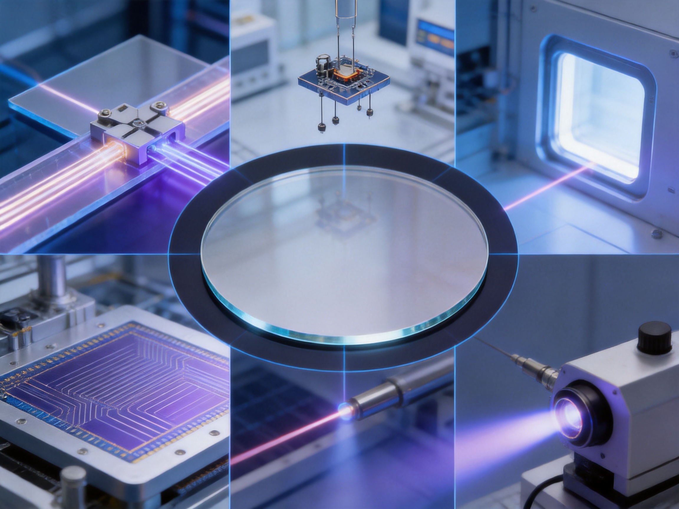
Customization begins with a review of the application and the customer’s technical drawing. The manufacturer can evaluate the desired diameter, thickness, tolerance, surface finish, edge geometry, locating features, optical grade, and packaging method.
Diameter and Thickness
Standard 2-inch, 4-inch, 6-inch, and 8-inch formats cover many laboratory and industrial requirements. Custom dimensions can be considered when the customer’s tool or assembly requires a different size. Thickness can also be customized to balance stiffness, weight, optical path length, thermal behavior, and handling strength.
Polishing Configuration
Single-sided polishing is appropriate when one surface is functional and the other is used as a support or mounting face. Double-sided polishing is preferred when both surfaces must be smooth or when parallelism and thickness uniformity are critical.
Edge and Orientation Features
Locating edges, orientation flats, chamfers, and C-shaped edges can be designed around the customer’s handling system. The position and dimensions of these features should be shown clearly on the drawing to avoid orientation errors during production.
Material Alternatives
Although the product is generally specified as a quartz wafer, material selection should be confirmed before mass production. The supplied technical information also refers to sapphire wafer customization, which indicates that the manufacturer has experience with other precision wafer materials. Quartz and sapphire have different optical, thermal, mechanical, and processing characteristics, so they should not be treated as interchangeable. The customer should identify the required material explicitly in the inquiry.
Inspection and Documentation
Customers may request dimensional reports, surface inspection results, roughness data, flatness measurements, material certificates, packing specifications, or first-article approval documentation. Defining the inspection method and acceptance criteria before production helps ensure that the delivered wafer is evaluated according to the customer’s actual process needs.
How to Select the Correct Quartz Wafer
The first step is to define the application environment. Important factors include wavelength, temperature range, chemical exposure, vacuum conditions, mechanical loading, electrical requirements, and expected service life. A wafer for ultraviolet spectroscopy may require a different material grade and surface specification from a wafer intended for MEMS bonding.
Next, determine the dimensional requirements. Diameter and thickness should match the equipment, carrier, chuck, or assembly. If the wafer will be handled automatically, orientation and edge features must be specified. If it will be diced or bonded, the customer should consider edge strength, thickness uniformity, and surface cleanliness.
Surface specifications should be selected according to the final function. Optical windows generally require surface quality and transmission data. Coating and lithography processes require roughness, flatness, and cleanliness control. Bonding processes may require carefully controlled roughness on both surfaces and strict particle limits.
Customers should also identify whether the product is for prototype development, low-volume production, or continuous mass production. Prototype projects may prioritize flexibility and engineering support, while volume programs require stable process capability, lot-to-lot consistency, packaging control, and dependable delivery schedules.
Packaging, Handling, and Storage
Quartz wafers should be handled by their edges using clean gloves or suitable wafer tools. Contact with the polished surface can leave fingerprints, organic residues, or particles that may affect subsequent processing. Even a hard material such as quartz can be scratched by inappropriate tools or contact with abrasive particles.
Protective packaging should separate individual wafers and prevent movement during transportation. Clean containers, protective films, wafer boxes, or custom fixtures may be selected according to the surface quality and cleanliness requirement. Packaging should also protect the edge because edge chips are a common source of damage during shipment.
Storage conditions should be dry, clean, and free from corrosive vapors. If the wafer is intended for semiconductor or optical coating processes, it should remain sealed until it enters the controlled processing area. Before use, the customer should follow an approved cleaning and inspection procedure appropriate to the material and application.
Why Work with an Experienced Custom Manufacturer?
A custom quartz wafer project involves more than cutting a circle from a glass plate. The final result depends on material selection, process sequencing, equipment capability, inspection accuracy, and communication between the manufacturer and the customer.
An experienced optical manufacturer can help identify conflicts between requirements. For example, a very thin large-diameter wafer may be difficult to handle if the flatness tolerance is extremely tight. A demanding optical surface may require additional polishing time and special cleaning. A chamfer designed for one carrier may not fit another. Early technical discussion can prevent costly redesigns and improve manufacturing efficiency.
Changzhou Haolilai Photo-Electricity Scientific and Technical Co., Ltd. combines optical-component manufacturing experience with custom engineering support. Its years of operation, broad product range, technical centers, quality certifications, patents, and export experience support both standard and project-specific requirements.
The company’s expertise in laser, automotive, semiconductor, and consumer optics also provides a broader understanding of how a wafer will be used after delivery. This application awareness can be valuable when the customer needs advice on surface quality, edge design, material choice, or inspection documentation.
Quality Assurance from Prototype to Production
Quality assurance should be considered throughout the manufacturing cycle rather than only at final inspection. Material approval, process planning, equipment maintenance, operator training, in-process measurement, environmental control, and final verification all contribute to product consistency.
For a new design, first-article samples can be used to confirm dimensions, surface condition, compatibility with the customer’s process, and packaging performance. Feedback from the initial batch can then be used to refine the drawing or establish a production control plan.
For repeat orders, traceability and documented procedures help maintain consistency between lots. Important controls may include material batch identification, polishing parameters, cleaning records, inspection results, and nonconformance management. These practices are especially important for semiconductor, automotive, and other regulated industries.
ISO 9001:2015 provides a framework for quality management, while ISO 14001:2015 supports environmental management. IATF 16949 experience is relevant to customers who require automotive-oriented process discipline and supplier quality controls. Certification does not replace product-specific technical verification, but it provides a structured basis for managing production and continuous improvement.
Frequently Asked Questions
What are quartz wafers mainly used for?
Quartz wafers are used in PLC planar waveguide splitter chips, MEMS devices, semiconductor research and manufacturing, laser optics, spectroscopy, imaging, optical communication, sensors, and other photonic applications. Their low thermal expansion, optical transmission, chemical resistance, and electrical insulation make them suitable for demanding environments.
What standard wafer diameters are available?
Common diameters include 2 inches, 4 inches, 6 inches, and 8 inches. The corresponding reference diameters are approximately 50.8 mm, 100 mm, 150 mm, and 200 mm. Other sizes can be considered for custom projects.
Can the thickness be customized?
Yes. Standard thicknesses include approximately 430 µm for 2-inch wafers, 650 µm for 4-inch wafers, and 1300 µm for 6-inch and 8-inch wafers. Custom thicknesses can be discussed, including designs of 0.1 mm or greater when the diameter, flatness, and mechanical requirements are feasible.
Are both sides polished?
The wafers can be supplied with double-sided polishing or polishing on one side. The appropriate option depends on whether both surfaces are functional, whether parallelism is critical, and whether the reverse side will be mounted or supported.
What surface roughness can be achieved?
The stated reference specification is Ra ≤ 0.3 nm. The required roughness should be confirmed for the selected material, diameter, polishing configuration, and application. Additional surface requirements may apply for bonding, lithography, laser optics, or semiconductor processing.
What does a 20/10 surface quality mean?
It is an optical surface-quality designation used to control scratches and digs. The exact inspection method and acceptance criteria should be confirmed in the technical specification. Customers with demanding optical applications may also need to define transmission, inclusions, haze, wedge, and wavefront requirements.
Can the wafer include a locating edge?
Yes. Round wafers can be supplied with locating edges or other orientation features. A 45-degree chamfer or C-shaped edge can also be specified. The customer should provide the required position and dimensions if the wafer must fit automated handling equipment.
Are quartz and sapphire wafers the same?
No. Quartz and sapphire are different materials with different optical transmission ranges, thermal behavior, hardness, chemical properties, and processing characteristics. The technical information includes a reference to customizable sapphire wafers, but the required material should be confirmed clearly before quotation and production.
Which material sources are available?
Quartz wafers may be manufactured from materials supplied by recognized sources such as Corning, Nikon, Heraeus, or other approved suppliers, depending on the required grade. Material availability and suitability should be confirmed according to wavelength, purity, thermal conditions, and processing requirements.
Can the manufacturer support prototypes?
Custom engineering support can be provided for prototype and production requirements. Customers should submit drawings or technical data covering diameter, thickness, tolerances, surface finish, edge profile, material, quantity, and inspection requirements.
What information should be included in an inquiry?
An inquiry should include the material, diameter, thickness, tolerance, surface roughness, warpage or flatness, total thickness deviation, surface quality, polishing configuration, edge design, locating features, quantity, application, operating wavelength, and required documentation. This information allows the manufacturer to recommend a suitable process and prepare an accurate quotation.
How should quartz wafers be handled?
Handle wafers by the edge with clean gloves or approved tools. Avoid touching the polished faces, stacking unprotected wafers, placing them on abrasive surfaces, or exposing them to uncontrolled contamination. Use suitable protective packaging and follow the cleaning procedure required for the final application.
Can quartz wafers be used in ultraviolet systems?
Yes. Quartz offers useful ultraviolet transmission and is widely used in ultraviolet optical components, spectroscopy, lithography, sensors, and laser systems. The actual performance depends on the quartz grade, wavelength, thickness, surface quality, and any applied coating.
Why is low warpage important?
Low warpage helps the wafer sit uniformly on processing stages, vacuum chucks, bonding fixtures, and inspection platforms. It can improve exposure focus, coating uniformity, bonding contact, alignment, and measurement repeatability.
Conclusion
High-precision quartz wafers provide an effective combination of optical transmission, low thermal expansion, mechanical stability, chemical resistance, electrical insulation, and precision surface control. These properties make them valuable in photonics, PLC devices, MEMS, semiconductor manufacturing, laser systems, spectroscopy, imaging, and scientific instrumentation.
Standard 2-inch, 4-inch, 6-inch, and 8-inch wafers are available with controlled diameter, thickness, roughness, warpage, thickness deviation, surface quality, polishing configuration, and edge geometry. Custom sizes, thicknesses, material grades, locating features, and inspection requirements can be evaluated for specialized projects.
With manufacturing experience dating back to 1998, a large precision optics facility, more than 300 employees, technical research centers, international supply experience, and ISO 9001:2015, ISO 14001:2015, and IATF 16949 certifications, Changzhou Haolilai Photo-Electricity Scientific and Technical Co., Ltd. is positioned to support customers from prototype development through repeat production.
The best wafer specification is determined by the complete application rather than by diameter alone. By defining the optical wavelength, process environment, dimensional tolerances, surface requirements, edge design, and inspection criteria at the beginning of the project, customers can obtain a quartz wafer that integrates reliably into their equipment and manufacturing process.
References
1. ISO 10110, Optics and Photonics — Preparation of Drawings for Optical Elements and Systems.
2. ISO 9001:2015, Quality Management Systems — Requirements.
3. ISO 14001:2015, Environmental Management Systems — Requirements with Guidance for Use.
4. IATF 16949, Quality Management System Requirements for Automotive Production and Relevant Service Parts Organizations.
5. Optical Materials and Their Applications, technical reference literature on fused silica, quartz, and precision optical substrates.
6. Semiconductor and MEMS Manufacturing Materials, technical reference literature on wafer processing, surface preparation, bonding, and contamination control.


 苏公网安备32041102000130号