
 Search
 en
en English
 日本語
日本語 русский
 Español
 Deutsch
 中文简体
中文简体Content
- 1 Introduction
- 2 What Is a Glass Wafer?
- 3 Key Advantages of Precision Glass Wafers
- 4 Available Sizes and Technical Specifications
- 5 Glass Materials for Different Applications
- 6 Advanced Manufacturing Process
- 7 Applications in Semiconductor and Electronics Manufacturing
- 8 Applications in Optics and Scientific Research
- 9 Advantages Over Conventional or Less Specialized Substrates
- 10 Company Manufacturing Strengths and Quality System
- 11 Customization and Engineering Support
- 12 How to Select the Right Glass Wafer
- 13 Frequently Asked Questions
- 13.1 What sizes of glass wafers are available?
- 13.2 What is the minimum thickness?
- 13.3 Which materials can be used?
- 13.4 Can glass wafers include locating edges or angles?
- 13.5 What edge treatments are available?
- 13.6 What surface roughness can be achieved?
- 13.7 What do the 20/10 surface specifications mean?
- 13.8 Are the wafers suitable for MEMS bonding?
- 13.9 Can the wafers be used for optical components?
- 13.10 How can customers request a quotation?
- 14 Conclusion
- 15 References
- 16 Product: Glass Wafer
Introduction
Glass wafers are essential engineering substrates for semiconductor packaging, microelectromechanical systems, optical components, sensor platforms, communications equipment, and scientific instruments. Their combination of optical transparency, chemical stability, dimensional consistency, thermal-shock resistance, and low alkali content makes them suitable for processes that demand clean surfaces and reliable performance. As electronic and optical devices become smaller and more complex, the quality of the substrate increasingly affects the quality, yield, and service life of the final product.
Changzhou Haolilai Photo-Electricity Scientific and Technical Co., Ltd. specializes in the production of high-precision glass wafers for industrial and research applications. The company supplies standard wafer sizes from 4 inches to 12 inches, while also supporting customized diameters, thicknesses, edge profiles, materials, and surface requirements. Its product range includes glass wafers made from Sodalime, Pyrex, Borofloat, borosilicate glass such as D263T, Corning Eagle XG, BK7, and other optical or technical glass materials selected according to application requirements.
The available glass wafers are designed for customers who need a stable and uniform platform for thin-film deposition, lithography, etching, bonding, optical fabrication, sensor assembly, or precision inspection. Standard specifications include a diameter tolerance of approximately ±0.1 mm, surface roughness as low as Ra ≤ 1 nm, warpage of no more than 10 µm, flatness of no more than 3 µm, and a 20/10 surface quality designation. These characteristics help improve process consistency and reduce the risks associated with surface defects, dimensional variation, and thermal instability.
This article explains the technical characteristics, manufacturing strengths, application benefits, customization capabilities, and quality considerations associated with high-precision glass wafers. It also compares the practical advantages of precision glass substrates with less specialized alternatives and provides a detailed question-and-answer section for engineers, purchasers, and product designers.
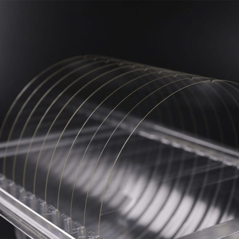
Glass Wafer
What Is a Glass Wafer?
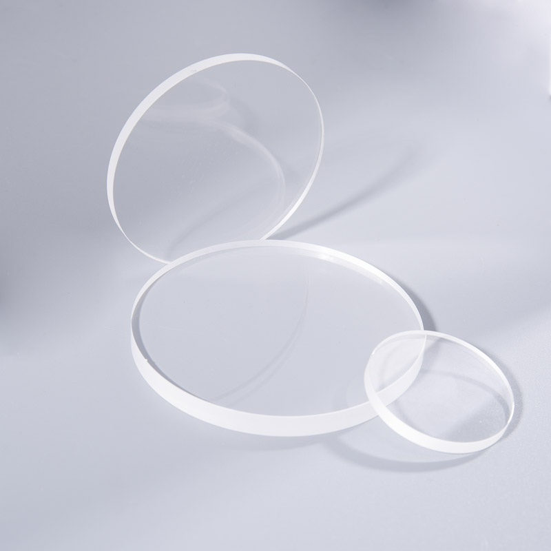
A glass wafer is a thin, flat, precision-manufactured glass substrate, normally produced in a circular form and sometimes supplied with a locating edge, locating angle, or other orientation feature. Unlike a finished semiconductor wafer made from silicon, a glass wafer generally functions as a transparent, electrically insulating, chemically stable, and mechanically consistent platform for subsequent processing.
Depending on the material and intended use, a glass wafer may serve as a carrier, temporary bonding substrate, optical reference surface, microfluidic platform, sensor substrate, packaging component, or base for deposited films and patterned structures. Its role is particularly important in processes where transparency is needed for alignment, inspection, ultraviolet exposure, optical measurement, or backside illumination.
The production of a high-quality glass wafer involves more than simply cutting a circular shape from a sheet of glass. The material must be selected for its thermal expansion, chemical resistance, optical transmission, alkali content, hardness, and compatibility with the customer’s process. The wafer must then be shaped, ground, polished, cleaned, inspected, and packaged in a way that protects its precision surface.
For demanding semiconductor and optical applications, the critical properties are often interdependent. For example, a polishing process must reduce roughness without creating subsurface damage. Edge treatment must remove chipping risks without reducing the usable area. Cleaning must remove particles and residues while avoiding chemical attack. Packaging must preserve the surface condition during storage and transportation.
Key Advantages of Precision Glass Wafers
Excellent Optical Transparency
One of the most important advantages of glass is its ability to transmit visible, near-infrared, ultraviolet, or other selected wavelengths, depending on its composition and thickness. Transparent substrates allow engineers to observe structures from the backside, align layers through the material, inspect bonding interfaces, and integrate optical functions into compact systems.
In optical manufacturing, transparency and homogeneity are fundamental to the production of lenses, filters, mirrors, windows, and sensor assemblies. A carefully selected glass wafer can provide a consistent optical path and reduce unwanted distortion caused by local variations in refractive index or thickness.
Low Fluorescence Intensity
Low fluorescence intensity is beneficial in imaging, analytical instruments, biological detection, and other applications that depend on a clean optical signal. Excessive fluorescence from a substrate can create background noise and reduce measurement accuracy. Technical glass materials selected for high-quality wafer production can help maintain a clearer signal, particularly when the substrate is exposed to energetic light or used near sensitive detectors.
Low and Controlled Thermal Expansion
Thermal expansion affects alignment, bonding, deposition, lithography, and long-term dimensional stability. A glass wafer with a suitable expansion coefficient can reduce dimensional changes during heating and cooling cycles. This is especially important in MEMS fabrication, sensor packaging, thin-film processing, and applications that join glass with silicon, ceramics, metals, or other materials.
Controlled thermal behavior also helps reduce stress at interfaces. When two materials with significantly different expansion coefficients are bonded together, temperature changes can generate tensile or compressive forces. Choosing a glass with an appropriate thermal expansion coefficient can reduce the probability of warpage, delamination, cracking, or alignment drift.
Strong Thermal-Shock Resistance
Glass wafers used in industrial processing may experience rapid temperature changes during cleaning, coating, baking, bonding, annealing, or inspection. Strong thermal-shock resistance helps the substrate tolerate these transitions without cracking or developing unacceptable deformation.
Thermal-shock performance depends on material composition, thickness, edge condition, internal stress, and processing quality. A precision wafer with properly finished edges and controlled internal characteristics is generally more reliable than a wafer produced from an unsuitable or poorly processed glass sheet.
Positive Chemical Stability
Glass provides a chemically stable surface for many deposition, lithography, etching, cleaning, and bonding processes. Depending on the selected grade, it can resist common chemicals and maintain its dimensional and surface characteristics during repeated processing steps.
Chemical stability is particularly valuable in semiconductor and MEMS production, where the substrate may be exposed to solvents, acids, alkaline solutions, plasma environments, photoresist materials, cleaning agents, and thin-film precursors. The exact compatibility must always be verified against the customer’s process conditions, but the wide range of available glass compositions allows engineers to select a suitable material for many environments.
Scratch Resistance and Surface Durability
A low-defect surface is essential for reliable wafer handling and process yield. Scratches can become initiation points for cracks, interfere with thin-film uniformity, create optical scatter, or produce defects during bonding. Proper grinding and polishing help create a smooth surface with controlled roughness and reduced defect density.
The supplied glass wafers can achieve a surface roughness of Ra ≤ 1 nm and a surface quality of 20/10 under applicable inspection conditions. These specifications indicate a high level of surface control for applications requiring precision contact, optical clarity, or uniform film deposition. Actual acceptance criteria can be adjusted according to the customer’s drawings and inspection standards.
Low Alkali Content Options
Low alkali glass is useful in electronic and optical environments where mobile ions could affect device performance, film adhesion, electrical insulation, or long-term stability. Selecting a low-alkali or specially formulated glass can reduce the risk of ion migration and contamination in sensitive processes.
This feature is relevant to semiconductor packaging, display-related technologies, sensor systems, and high-temperature thin-film applications. Material selection should be based on the complete process flow, including temperature, humidity, electrical field, chemical exposure, and storage conditions.
Available Sizes and Technical Specifications
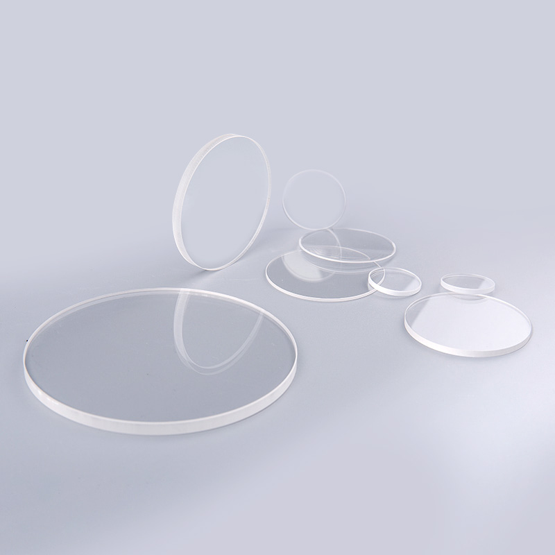
The standard product range includes 4-inch, 5-inch, 6-inch, 8-inch, and 12-inch glass wafers. These sizes correspond to commonly used laboratory, industrial, semiconductor, optical, and packaging platforms. The company can also discuss other dimensions and nonstandard configurations for customers with specialized equipment or product designs.
| Specification | 4 Inch | 5 Inch | 6 Inch | 8 Inch | 12 Inch |
|---|---|---|---|---|---|
| Nominal Diameter | 100 mm | 125 mm | 150 mm | 200 mm | 300 mm |
| Diameter Tolerance | 100 ± 0.1 mm | 125 ± 0.1 mm | 150 ± 0.1 mm | 200 ± 0.1 mm | 300 ± 0.1 mm |
| Typical Thickness | 500 ± 5 µm | 625 ± 5 µm | 675 ± 5 µm | 725 ± 5 µm | 900 ± 5 µm |
| Thickness Option | Customized available | Customized available | Customized available | Customized available | Customized available |
| Surface Roughness | Ra ≤ 1 nm | Ra ≤ 1 nm | Ra ≤ 1 nm | Ra ≤ 1 nm | Ra ≤ 1 nm |
| Warpage | ≤ 10 µm | ≤ 10 µm | ≤ 10 µm | ≤ 10 µm | ≤ 10 µm |
| Flatness | ≤ 3 µm | ≤ 3 µm | ≤ 3 µm | ≤ 3 µm | ≤ 3 µm |
| Surface Quality | 20/10 | 20/10 | 20/10 | 20/10 | 20/10 |
The values in the table represent typical standard specifications. Actual tolerances may vary according to material, diameter, thickness, processing method, inspection equipment, and customer requirements. Customized tolerances can be evaluated during technical communication and quotation.
Glass Materials for Different Applications
Sodalime Glass
Sodalime glass is widely available and can be a practical choice for applications that require a transparent, economical, and stable substrate. It is suitable for certain laboratory platforms, general optical components, educational devices, and applications where extreme thermal or chemical performance is not required.
When using Sodalime glass in a process, engineers should evaluate its thermal expansion, alkali content, temperature range, and chemical compatibility. It may be appropriate for cost-sensitive applications, while more demanding semiconductor or thermal-cycle environments may require a borosilicate or specialized optical glass.
Pyrex and Borofloat
Pyrex and Borofloat-type borosilicate materials are valued for their relatively low thermal expansion, good thermal-shock resistance, and chemical durability. They are commonly considered for laboratory equipment, MEMS structures, bonded assemblies, optical platforms, and processes that involve heating and cooling.
These materials can provide a useful balance between performance and cost. Their thermal characteristics are often better suited to precision processing than those of ordinary soda-lime glass, particularly when dimensional stability is important.
Borosilicate Glass such as D263T
D263T and similar borosilicate materials are used in precision technical applications where thinness, surface quality, chemical stability, and optical performance must be considered together. Such glass can be suitable for sensor covers, microfabricated structures, optical windows, and electronic components.
The specific grade should be selected according to wavelength transmission, thermal expansion, softening temperature, chemical exposure, and bonding method. A material data review before production can help ensure compatibility with the customer’s process.
Corning Eagle XG
Corning Eagle XG is a technical glass associated with demanding electronic and display-related applications. Its low-alkali characteristics and dimensional stability can be useful where contamination control and thermal performance are important.
When this material is specified, the wafer manufacturing process must preserve the original material’s advantages. Surface cleanliness, edge integrity, thickness uniformity, and packaging quality all influence the performance of the finished substrate.
BK7 Optical Glass
BK7 is a well-known optical glass used in lenses, prisms, windows, and other precision optical components. It offers useful optical homogeneity and transmission characteristics for many visible and near-infrared applications.
BK7 glass wafers can serve as optical reference substrates, filter bases, sensor windows, or starting blanks for further optical processing. The required flatness, parallelism, surface quality, and coating compatibility should be defined according to the final optical design.
In addition to the listed materials, the company can review requests for custom glass compositions. Material availability and processing feasibility depend on the required dimensions, tolerances, surface condition, thermal properties, and order quantity.
Advanced Manufacturing Process
Material Selection and Incoming Inspection
Manufacturing begins with the selection of a glass grade that matches the application. Key factors include optical transmission, refractive index, thermal expansion coefficient, chemical resistance, alkali content, hardness, internal stress, and temperature tolerance.
Incoming material inspection may include dimensional checks, visual examination, surface evaluation, and verification of material documentation. Careful selection at this stage helps prevent downstream problems such as excessive chipping, poor polishing response, thermal cracking, or incompatibility with the customer’s process.
Precision Cutting and Wafer Shaping
Glass sheets or blanks are cut into circular substrates using controlled cutting and shaping methods. The cutting process must limit edge damage and avoid introducing excessive mechanical stress into the material. Diameter tolerance is controlled according to the required wafer size and the customer’s equipment interface.
For semiconductor-style handling, wafers may be supplied with locating edges or locating angles. These orientation features help automated equipment identify wafer direction and maintain alignment during processing. The shape and position of such features can be customized when required by a particular tool or production line.
Edge Grinding and Inverted-Edge Processing
Edges are among the most vulnerable areas of a glass wafer. Sharp or damaged edges can produce particles, cause handling injuries, interfere with automated equipment, or become starting points for cracks. Edge grinding and finishing are therefore important parts of the manufacturing process.
Available edge configurations include 45-degree inverted edges, SEMI-style edge profiles, and C-shaped edge treatments. The appropriate profile depends on the wafer thickness, handling method, process equipment, and mechanical requirements. A properly finished edge improves handling safety and reduces the risk of chipping during transportation and processing.
Grinding and Thickness Control
Grinding establishes the basic thickness, parallelism, and flatness of the wafer. It must be carefully controlled because excessive material removal or uneven mechanical pressure can create warpage and internal stress.
The standard thicknesses range from approximately 500 µm for 4-inch wafers to approximately 900 µm for 12-inch wafers, with customized thicknesses available. Thickness tolerance may be adjusted to meet the needs of bonding, optical transmission, mechanical strength, or equipment compatibility.
Precision Polishing
Polishing produces the smooth, low-roughness surface required for thin-film deposition, optical inspection, bonding, and microfabrication. The process is designed to reduce grinding marks, scratches, haze, and subsurface damage while maintaining the required flatness.
A surface roughness of Ra ≤ 1 nm is available for the listed standard sizes. Such a smooth surface supports better film uniformity and reduces the likelihood that microscopic surface features will affect bonding or optical performance. For applications with special requirements, single-side polishing, double-side polishing, or other surface treatments can be discussed.
Cleaning and Contamination Control
After mechanical processing, the wafer surface must be cleaned to remove particles, polishing residues, oils, and other contaminants. Cleaning procedures are selected according to the glass material and final use. Proper rinsing and drying are necessary to prevent stains, residues, and water marks.
Contamination control is especially important for semiconductor and MEMS applications. Particles can affect lithography, deposition, bonding, and electrical performance. A clean surface also improves the reliability of optical inspection and subsequent coating processes.
Inspection and Measurement
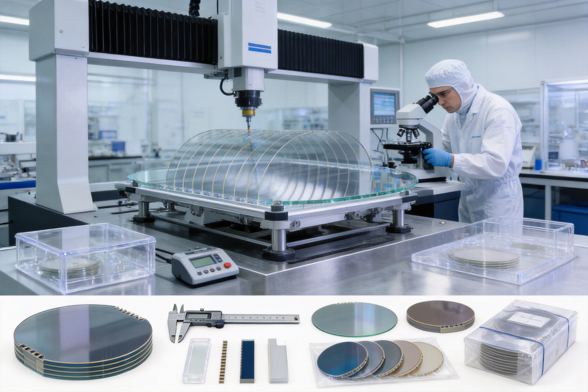
Inspection verifies that the finished wafer meets dimensional and surface requirements. Typical evaluation items include diameter, thickness, thickness variation, flatness, warpage, edge profile, surface roughness, scratches, digs, chips, particles, and visual defects.
Measurement results can be documented according to customer requirements. For high-precision orders, inspection planning may include sampling procedures, defined measurement locations, acceptance criteria, and quality records. This approach helps customers integrate the glass wafers into their quality management and incoming inspection systems.
Protective Packaging
Even a precisely polished wafer can be damaged by poor packaging. Finished wafers are protected against contact, vibration, particles, humidity, and impact during storage and transportation. Packaging design may vary according to wafer diameter, thickness, surface finish, shipping distance, and customer handling method.
Protective packaging is part of product quality rather than an afterthought. It helps ensure that the wafer received by the customer retains the surface condition and dimensional integrity achieved during production.
Applications in Semiconductor and Electronics Manufacturing
Integrated Circuit and Advanced Packaging Substrates
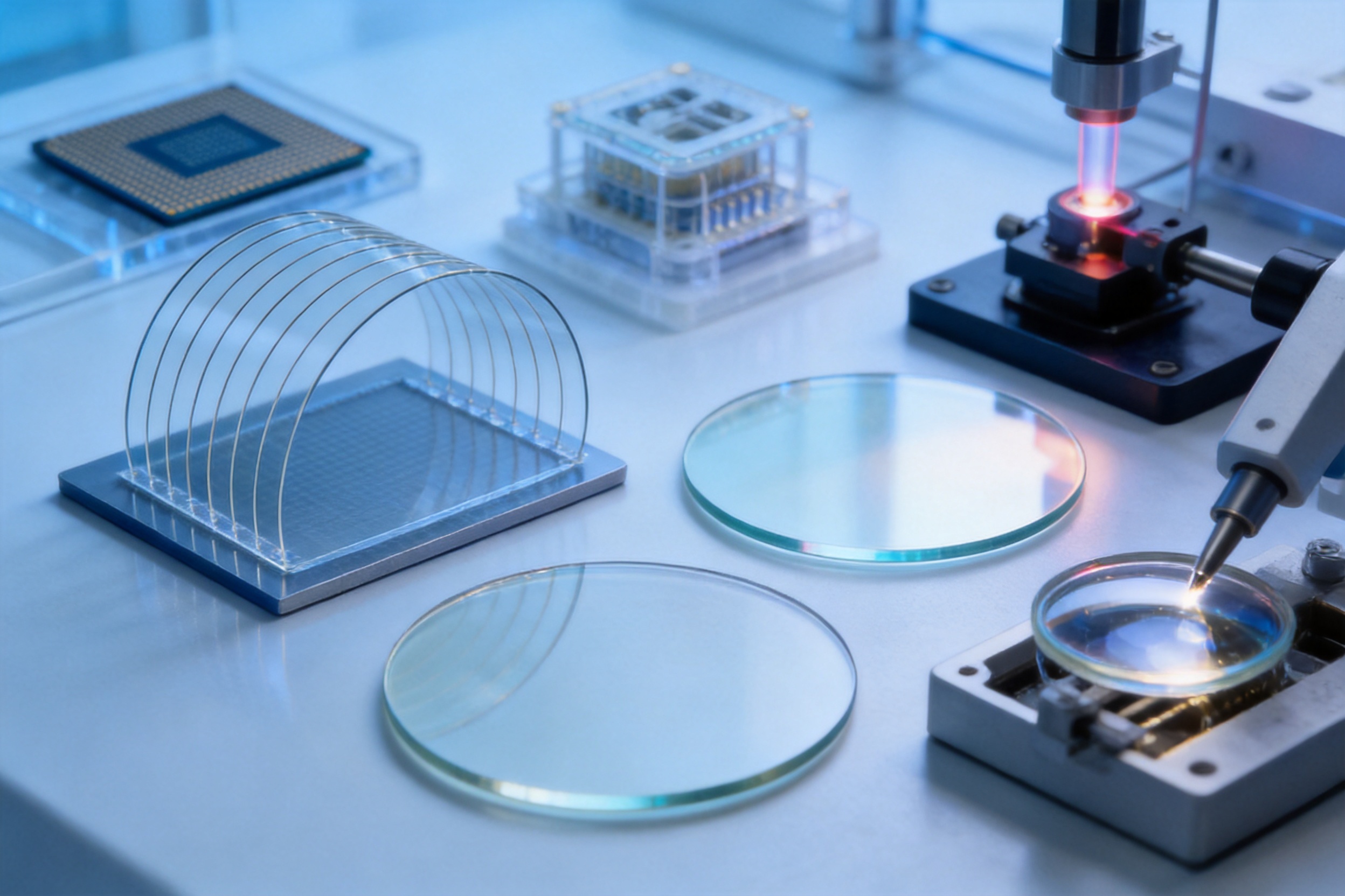
Glass wafers can be used as substrates or carriers in integrated circuit packaging and advanced assembly processes. Their flat, stable surfaces support redistribution layers, thin-film deposition, bonding, lithography, and temporary carrier technologies.
Glass is electrically insulating and transparent, which can provide design flexibility in packaging structures. Its surface can be patterned or coated, and its thermal behavior can be selected to improve compatibility with other materials. In some applications, a glass carrier supports thin components during processing and is later separated or reused.
MEMS Fabrication
MEMS devices often include microscopic mechanical structures, sensors, actuators, channels, and cavities. Glass wafers can be used as structural substrates, bonding partners, capping layers, or transparent inspection platforms.
In anodic bonding and related processes, the glass composition, surface flatness, cleanliness, and thermal expansion must be carefully controlled. A uniform glass wafer can improve bonding contact and reduce voids. Transparency allows engineers to inspect internal structures and bonding quality without immediately destroying the assembly.
Sensor Packaging
Glass wafers are used in the packaging of pressure sensors, optical sensors, image sensors, chemical sensors, and other electronic devices. The material can provide environmental protection while maintaining optical or mechanical access to the sensing element.
Low fluorescence, low alkali content, and chemical stability are valuable for sensors that operate near light-sensitive or chemically active components. The final design may require coatings, apertures, etched cavities, or precise alignment features, all of which can be considered during customization.
Communication and Data Processing Equipment
High-speed communications and data-processing systems increasingly rely on optical and electronic integration. Glass substrates can support optical paths, alignment structures, photonic elements, and packaging assemblies.
The transparency and dimensional stability of glass can simplify optical alignment and enable compact designs. A controlled surface also supports the application of antireflection coatings, conductive films, dielectric layers, or other functional coatings.
Applications in Optics and Scientific Research
Optical Windows and Filters
Glass wafers can be used as starting substrates for optical windows and filters. Their surfaces may be polished, coated, etched, or assembled into a larger optical system. The selected material determines transmission range, refractive index, dispersion, thermal response, and environmental durability.
For imaging systems, cameras, telescopes, laser equipment, and measurement instruments, surface quality and flatness are critical. Small defects can scatter light or reduce contrast, while nonuniform thickness can introduce wavefront distortion. Precision glass wafer processing helps establish a consistent base for later optical finishing.
Optical Lenses, Mirrors, and Prisms
Glass wafers can be used as blanks or substrates in the production of lenses, mirrors, and prisms. BK7 and other optical glasses may be selected when transmission, homogeneity, and refractive properties are important.
For reflective components, a glass substrate may receive a metal or dielectric coating. The substrate’s flatness, cleanliness, and thermal stability affect coating uniformity and long-term reliability. For transmissive components, the glass composition and surface quality influence the final optical performance.
Laser Systems
Laser systems require optical materials with stable transmission, low scatter, and reliable surface quality. Glass wafers may be used in beam paths, protective windows, alignment structures, filter assemblies, and coated optical elements.
Material selection must consider the operating wavelength, laser power, coating design, thermal load, and environmental conditions. Low-defect surfaces are particularly important because scratches, digs, or contamination can increase scatter and reduce the service life of the component.
Research and Laboratory Platforms
Universities, research laboratories, and development teams use glass wafers for experiments involving microfluidics, thin films, surface chemistry, optical measurements, biological analysis, and nanofabrication. Standard sizes help researchers work with established equipment, while custom sizes support experimental platforms and prototypes.
Because glass is transparent and chemically stable, researchers can observe reactions, fluid movement, deposited films, and microstructures directly through the substrate. This makes glass wafers useful for both development and educational environments.
Advantages Over Conventional or Less Specialized Substrates
The most important advantage of a precision glass wafer is the combination of properties rather than any single specification. A basic glass disc may offer transparency, but it may not provide the controlled flatness, low roughness, edge quality, cleanliness, and dimensional accuracy needed for semiconductor or optical processing.
Compared with ordinary cut glass, precision wafers offer improved control over diameter, thickness, warpage, flatness, and surface condition. These improvements can reduce alignment errors, improve coating uniformity, and lower the risk of breakage during handling.
Compared with some opaque substrates, glass enables backside inspection and optical alignment. This can simplify process development and quality control. It also makes glass attractive for systems in which light must pass through the substrate or in which the user needs to observe internal features.
Compared with materials that have higher thermal expansion or lower chemical stability, suitable glass grades can provide better dimensional consistency during temperature changes and chemical processing. This is valuable for bonded assemblies and multilayer structures.
The availability of several glass families is another advantage. Customers are not limited to one general-purpose material. They can select Sodalime for economical applications, borosilicate glass for thermal and chemical performance, specialized low-alkali glass for electronic uses, or BK7 for optical requirements.
Customization further distinguishes precision glass wafer production from commodity supply. Diameter, thickness, orientation feature, inverted edge, surface roughness, flatness, polishing method, material, and packaging can be discussed as part of a technical solution rather than treated as fixed catalog limitations.
Company Manufacturing Strengths and Quality System
Changzhou Haolilai Photo-Electricity Scientific and Technical Co., Ltd. was founded in 1998 and is located in Changzhou, Jiangsu, China. The company operates from a facility covering approximately 35,000 square meters and employs more than 300 people. Its business focuses on precision optical components and related products for laser optics, automotive optics, semiconductor optics, and consumer optics.
The company has obtained ISO9001:2015 quality management certification, ISO14001:2015 environmental management certification, and IATF16949 certification. These systems support controlled production, traceability, process management, environmental responsibility, and automotive-industry quality requirements.
As a recognized high-technology enterprise in Jiangsu Province, the company maintains an experienced technical team and has established the Jiangsu Precision Optical Lens Engineering Technology Center and Jiangsu Enterprise Technology Research Center. Its technical activities include product development, process improvement, precision manufacturing, and optical engineering.
The company has obtained invention patents, utility model patents, and Jiangsu High and New Tech Product recognitions. It exports products to more than 20 countries and holds more than 30 certificates and patents. These capabilities support cooperation with customers that require stable supply, engineering communication, custom specifications, and international quality documentation.
For glass wafer customers, the practical value of this background lies in the combination of technical experience, manufacturing resources, quality controls, and application knowledge. A supplier that understands both optical components and semiconductor-related substrates can better evaluate the relationship between material, surface finish, geometry, packaging, and final application performance.
Customization and Engineering Support
Standard 4-inch, 5-inch, 6-inch, 8-inch, and 12-inch wafers are suitable for many applications, but specialized programs often require nonstandard designs. Custom glass wafers can be considered for other diameters, thicknesses, edge profiles, orientation features, roughness levels, flatness requirements, and surface quality grades.
Customers should provide drawings or technical information whenever possible. Useful details include nominal diameter, thickness, tolerance, single-side or double-side polishing, surface roughness, flatness, warpage, parallelism, edge treatment, locating feature dimensions, material grade, coating compatibility, packaging method, and inspection standard.
Process information is also valuable. The supplier should know whether the wafer will be exposed to high temperature, ultraviolet light, vacuum, plasma, acids, alkaline solutions, solvents, bonding pressure, or repeated thermal cycling. This information helps the engineering team recommend an appropriate glass material and manufacturing route.
For prototype projects, small-volume production, or research programs, customization can help reduce unnecessary cost and avoid forcing a nonstandard application into an unsuitable catalog specification. For high-volume programs, early technical communication can help establish repeatable tolerances, inspection procedures, packaging methods, and supply schedules.
How to Select the Right Glass Wafer
Define the Process Environment
Start by identifying the temperature range, chemical exposure, vacuum conditions, light wavelength, mechanical loads, and bonding method. These factors determine whether the application needs Sodalime, borosilicate, low-alkali glass, BK7, or another material.
Determine Dimensional Requirements
Define diameter, thickness, tolerance, flatness, warpage, and parallelism. If the wafer will be processed in semiconductor equipment, the dimensions and orientation features must match the tool specification. If it will be used as an optical component, thickness uniformity and surface flatness may be more important than standard handling features.
Specify Surface Requirements
Surface roughness and surface quality should be connected to the intended process. Thin-film deposition, direct bonding, optical transmission, and lithography may each require different surface conditions. A lower roughness may be beneficial, but it should be evaluated together with flatness, cleanliness, and cost.
Review Edge Geometry
Edge treatment affects mechanical safety and compatibility with handling equipment. A 45-degree inverted edge, SEMI-style edge, or C-shaped edge may be selected depending on the application. The edge profile should be included on the drawing to avoid ambiguity.
Confirm Inspection and Packaging
Before production, the customer and supplier should agree on measurement methods, sampling plans, surface inspection criteria, packaging, labeling, and documentation. Clear acceptance criteria help prevent misunderstandings and support stable repeat orders.
Frequently Asked Questions
What sizes of glass wafers are available?
Standard sizes include 4-inch, 5-inch, 6-inch, 8-inch, and 12-inch wafers. Other diameters can be evaluated as custom products according to material availability, manufacturing feasibility, and order requirements.
What is the minimum thickness?
The company specializes in high-precision glass wafers with a thickness of at least 0.1 mm. Standard catalog thicknesses are approximately 500 µm, 625 µm, 675 µm, 725 µm, and 900 µm for the listed wafer sizes. Custom thicknesses can be discussed.
Which materials can be used?
Available materials include Sodalime, Pyrex, Borofloat, borosilicate glass such as D263T, Corning Eagle XG, BK7, and other technical or optical glass materials. The best material depends on thermal, optical, chemical, electrical, and mechanical requirements.
Can glass wafers include locating edges or angles?
Yes. Wafers can be supplied as round substrates with locating edges or locating angles. The design can be adapted to the handling and alignment requirements of the customer’s equipment.
What edge treatments are available?
Available options include 45-degree inverted edges, SEMI-style edge profiles, and C-shaped edge treatments. Custom edge designs may be considered when drawings and application information are provided.
What surface roughness can be achieved?
The listed standard specification is Ra ≤ 1 nm. The final achievable value depends on the material, wafer size, polishing method, thickness, and inspection method. Special requirements should be confirmed before production.
What do the 20/10 surface specifications mean?
20/10 generally refers to an optical surface quality classification describing allowable scratch and dig levels under a specified inspection method. The exact interpretation should be confirmed with the supplier’s quality team and the customer’s inspection standard.
Are the wafers suitable for MEMS bonding?
Glass wafers can be suitable for MEMS bonding when the material, surface condition, flatness, cleanliness, and thermal expansion are compatible with the bonding process. Customers should provide details about anodic bonding, fusion bonding, adhesive bonding, or other methods so the wafer can be specified correctly.
Can the wafers be used for optical components?
Yes. Glass wafers can serve as substrates or blanks for lenses, mirrors, filters, windows, prisms, sensor covers, and laser-system components. Optical performance depends on the selected material, wavelength, surface quality, flatness, thickness uniformity, and any required coating.
How can customers request a quotation?
Customers can provide the required diameter, thickness, material, tolerances, surface specifications, edge design, quantity, application, and delivery requirements. Technical drawings, sample references, and process conditions are useful for preparing an accurate quotation.
Conclusion
High-precision glass wafers provide a reliable foundation for semiconductor packaging, MEMS fabrication, optical systems, sensor assemblies, communications equipment, and scientific research. Their main benefits include transparency, low fluorescence, controlled thermal expansion, thermal-shock resistance, chemical stability, scratch resistance, low alkali options, and compatibility with precision surface processing.
The product range described here combines standard wafer sizes with extensive customization possibilities. Diameters from 4 inches to 12 inches, thicknesses from approximately 0.1 mm upward, surface roughness as low as Ra ≤ 1 nm, flatness of no more than 3 µm, warpage of no more than 10 µm, and 20/10 surface quality provide a strong starting point for demanding technical applications.
Manufacturing quality depends on the entire production chain, including material selection, precision cutting, edge finishing, grinding, polishing, cleaning, inspection, and protective packaging. Changzhou Haolilai Photo-Electricity Scientific and Technical Co., Ltd. combines optical manufacturing experience, technical development resources, certified management systems, and international supply experience to support both standard and customized glass wafer programs.
By defining the material, geometry, surface condition, edge configuration, and process environment at the beginning of a project, customers can select a glass wafer that improves process stability and supports consistent final-product performance. For specialized requirements, the engineering team can review drawings and application details to develop a suitable manufacturing solution.
References
1. ISO 9001:2015, Quality Management Systems—Requirements.
2. ISO 14001:2015, Environmental Management Systems—Requirements with Guidance for Use.
3. IATF 16949, Quality Management System Requirements for Automotive Production and Relevant Service Parts Organizations.
4. Semiconductor Equipment and Materials International, Semiconductor Wafer and Substrate Handling Practices.
5. Optical Society of America, Optical Glass Properties and Precision Surface Quality Terminology.
6. ASTM International, Standards for Glass, Optical Materials, Surface Finish, and Dimensional Measurement.
7. Technical literature on borosilicate glass, thermal expansion, chemical durability, and glass-to-silicon bonding.
8. Technical literature on MEMS fabrication, anodic bonding, wafer-level packaging, and transparent substrate applications.


 苏公网安备32041102000130号