
 Search
 en
 English
 日本語
 русский
 Español
 Deutsch
 中文简体
Content
- 1 What Is a Sapphire Wafer?
- 2 Key Material Advantages of Sapphire
- 3 Precision Specifications and Product Configurations
- 4 Flatness, Warpage, and Surface Roughness
- 5 Surface Quality and Edge Design
- 6 Manufacturing Process for High-Precision Sapphire Wafers
- 7 Why Precision Manufacturing Matters
- 8 Advantages Over Alternative Substrate Materials
- 9 Application Areas
- 10 Customization Options
- 11 Company Manufacturing Strengths
- 12 Quality Management and Customer Support
- 13 How to Select the Right Sapphire Wafer
- 14 Frequently Asked Questions
- 14.1 What is the main advantage of a sapphire wafer?
- 14.2 What standard wafer diameters are available?
- 14.3 What thicknesses are available?
- 14.4 Can the wafers be supplied with special edges?
- 14.5 What are the stated flatness and warpage specifications?
- 14.6 What surface roughness can be achieved?
- 14.7 Are sapphire wafers electrically conductive?
- 14.8 Are sapphire wafers suitable for LED applications?
- 14.9 Can sapphire wafers be used in high-temperature environments?
- 14.10 How does sapphire compare with ordinary glass?
- 14.11 Can the company provide customized wafers?
- 14.12 What information should be included in an inquiry?
- 14.13 What industries does the manufacturer serve?
- 14.14 What quality certifications does the company hold?
- 14.15 How can customers request more information?
- 15 Conclusion
- 16 References
- 17 Product: Sapphire Wafer
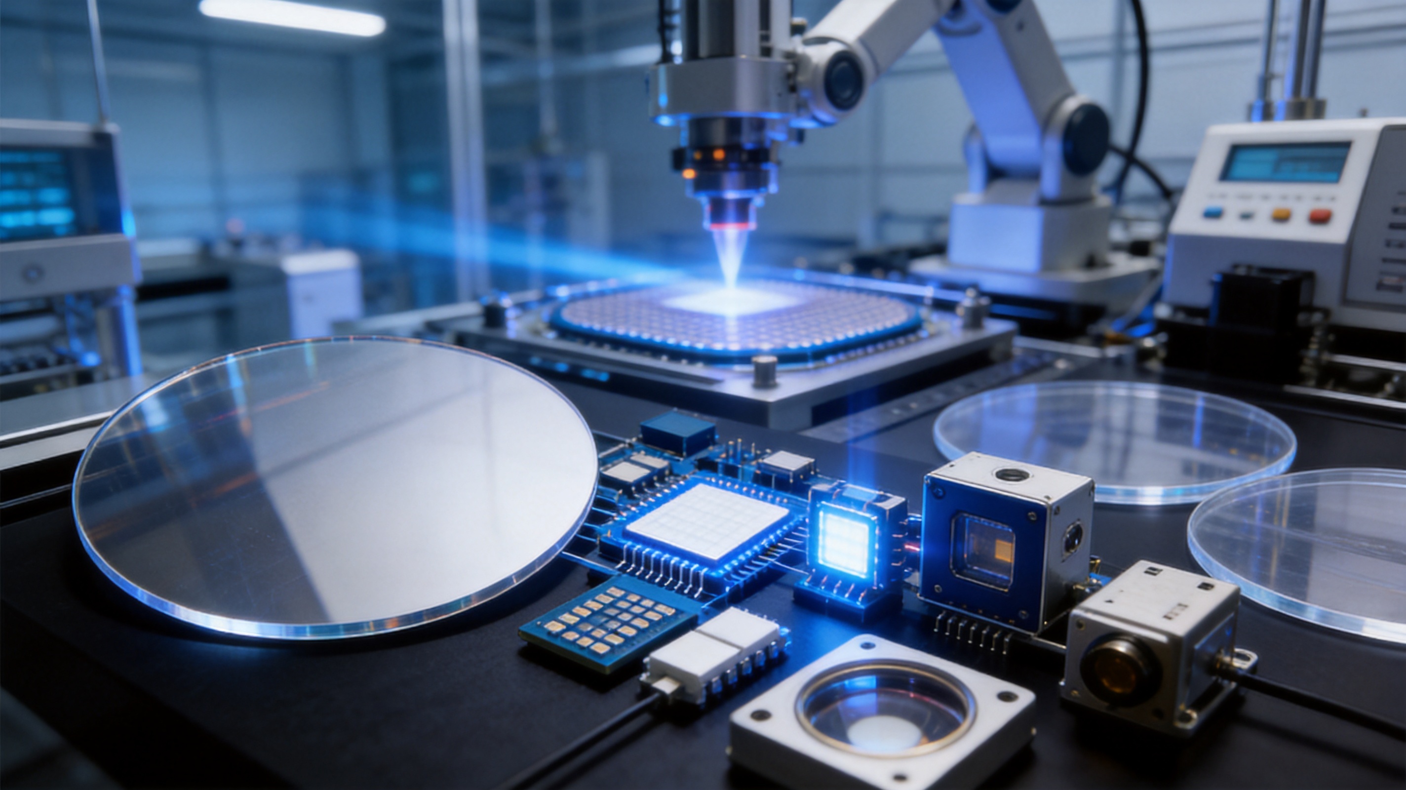
Sapphire wafers are among the most durable and versatile substrate materials used in modern semiconductor, optoelectronic, photonic, and electronic device manufacturing. Produced from single-crystal aluminum oxide, sapphire combines optical transparency, electrical insulation, mechanical strength, chemical stability, and high-temperature performance in one material platform. These properties make it suitable for applications in which ordinary glass, silicon, ceramic, or polymer substrates may not provide sufficient durability, purity, insulation, or environmental resistance.
High-precision sapphire wafers are particularly important in the production of semiconductor optoelectronic devices, light-emitting diodes, laser-related components, sensors, and other products that require a stable and reliable substrate. The wafer must not only possess the inherent properties of sapphire, but must also meet demanding dimensional and surface requirements. Diameter tolerance, thickness uniformity, flatness, warpage, surface roughness, edge geometry, and surface quality all influence the performance and yield of downstream manufacturing processes.
Changzhou Haolilai Photo-Electricity Scientific and Technical Co., Ltd. specializes in the production of precision optical and optoelectronic components, including sapphire wafers for industrial and advanced technology applications. With a manufacturing history beginning in 1998, the company serves customers in semiconductor optics, laser optics, automotive optics, consumer optics, and related fields. Its technical capabilities, quality management systems, research resources, and customization services support the production of wafers designed for demanding industrial environments.
What Is a Sapphire Wafer?
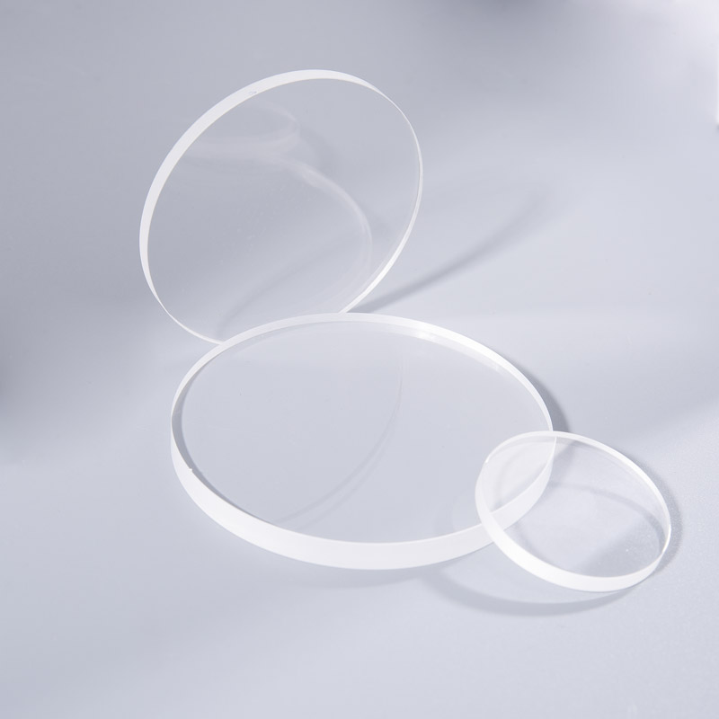
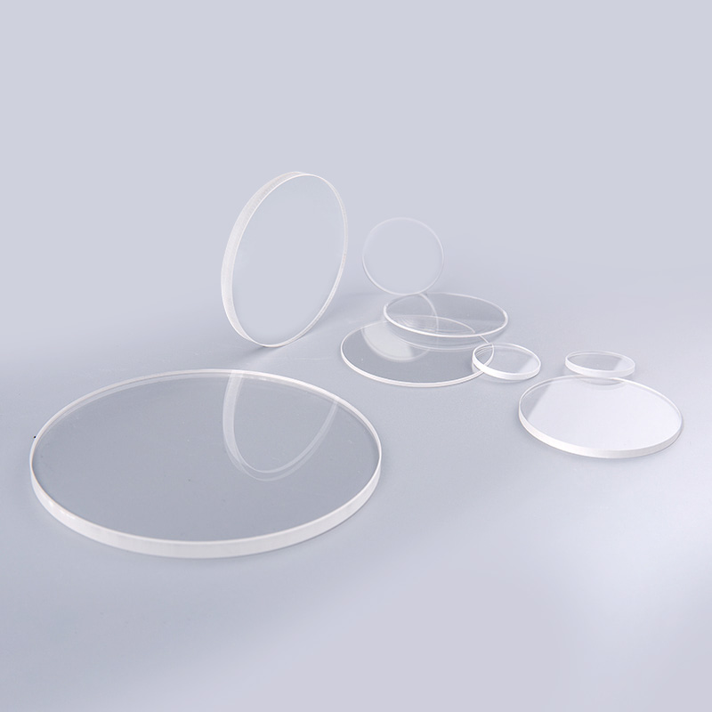
A sapphire wafer is a thin, precisely processed slice of single-crystal aluminum oxide. Although sapphire is widely known as a gemstone, industrial sapphire is valued primarily for its engineering characteristics rather than its decorative appearance. The crystal structure provides a combination of hardness, transparency, electrical insulation, and resistance to heat and chemicals that is difficult to obtain from a single alternative material.
In semiconductor and optoelectronic production, a sapphire wafer acts as a substrate. A substrate provides a stable surface on which other materials, semiconductor layers, electrodes, coatings, or functional structures can be deposited or fabricated. The substrate must remain dimensionally stable during processing, resist chemical and thermal exposure, and provide the required electrical or optical behavior.
Sapphire is especially useful when electrical isolation is required. Unlike conductive semiconductor substrates, sapphire effectively blocks current flow. This property helps isolate electronic devices and components from one another and can support the design of devices that require a nonconductive foundation. It can also reduce unwanted electrical interaction between the active device and the supporting substrate.
The term “wafer” generally refers to the circular form used in semiconductor processing, although wafers may also be supplied with locating edges, locating angles, or other orientation features. These features assist with alignment, handling, and process control. Depending on the customer’s requirements, sapphire wafers may be supplied in standard industrial diameters or produced in customized dimensions.
Key Material Advantages of Sapphire
Exceptional Hardness and Wear Resistance
Sapphire is one of the hardest naturally occurring engineering materials, ranking immediately after diamond according to the supplied product information. Its high hardness provides strong resistance to scratching, abrasion, and surface damage. This is especially beneficial during transportation, automated handling, device assembly, and operation in environments where particles or contact may damage softer materials.
Compared with ordinary glass, sapphire is substantially more resistant to scratching and mechanical wear. Compared with many transparent polymers, it offers superior dimensional stability and resistance to surface degradation. This makes sapphire suitable for products that must maintain optical or physical integrity over a long service period.
Hardness alone does not determine the performance of a wafer, but it provides an important foundation for reliability. A wafer with a scratch-resistant surface is less likely to develop defects during handling or subsequent processing. A durable surface may also reduce the risk of contamination caused by surface chipping, flaking, or abrasion.
High Mechanical Strength
Sapphire combines high hardness with strong mechanical performance. Its strength and impact resistance allow it to withstand demanding handling conditions more effectively than many conventional transparent materials. This is valuable in semiconductor and optoelectronic production, where wafers may pass through multiple cleaning, coating, inspection, alignment, and assembly stages.
Mechanical stability is also important when wafers are exposed to clamping, vacuum handling, thermal cycling, or process equipment. A precisely manufactured sapphire wafer can provide a stable platform for thin-film deposition and other high-accuracy processes. The specified control of warpage and flatness further supports reliable contact with equipment and uniform processing across the wafer surface.
Electrical Insulation
One of sapphire’s most important advantages over many semiconductor materials is its ability to electrically isolate devices and components. Sapphire is an electrically insulating substrate, making it suitable for applications in which conductive coupling between the device and the substrate would be undesirable.
Electrical isolation can simplify device architecture and help control leakage paths. It can also support the development of products that contain multiple electrically separate elements on the same supporting platform. For optoelectronic devices, sensors, and specialized electronic components, this characteristic can improve design flexibility and support stable operation.
Optical Transparency
Sapphire offers broad optical transparency in relevant wavelength ranges and is used in applications that require a clear, stable, and durable optical material. Its transparency, combined with its hardness and chemical resistance, makes it useful for optical windows, sensor covers, device substrates, and optoelectronic structures.
When a sapphire wafer is manufactured with controlled surface quality and low roughness, it can support applications in which light transmission, reflection, scattering, or optical alignment must be carefully managed. Surface quality specifications such as 20/10 provide a way to define allowable surface defects for precision applications.
High-Temperature Resistance
Sapphire maintains its performance in high-temperature environments and offers strong resistance to thermal degradation. This makes it appropriate for processes and applications involving elevated temperatures, thermal cycling, or hot operating environments.
High-temperature resistance is particularly relevant to semiconductor processing, where wafers may be exposed to heating, deposition, annealing, or other thermal operations. A substrate that maintains its shape and surface integrity during these stages can contribute to improved process repeatability and product reliability.
Chemical and Corrosion Resistance
Sapphire has strong resistance to corrosion and chemical attack in many industrial environments. This property allows it to function in applications involving cleaning agents, process chemicals, and other potentially aggressive substances. Chemical stability helps preserve surface condition and dimensional accuracy during repeated processing.
Compared with less durable materials, sapphire can offer a longer service life when exposed to moisture, abrasion, and chemical environments. The exact compatibility of sapphire with a particular chemical process should always be confirmed through application-specific testing, but its general chemical resistance is a major reason it is selected for demanding technical uses.
Biocompatibility
The supplied product information identifies biocompatibility as another desirable characteristic of sapphire. This expands its potential use beyond semiconductor and optical applications into specialized medical, analytical, and laboratory equipment. Where a stable, hard, electrically insulating, and chemically resistant material is needed, sapphire may provide an effective substrate or protective component.
Precision Specifications and Product Configurations
The performance of a sapphire wafer depends on both the raw crystal and the precision of the conversion process. A wafer must be cut, ground, polished, shaped, cleaned, and inspected to meet the dimensional requirements of the intended application. The available product range includes standard wafer diameters from four inches to twelve inches, together with customized options.
| Specification | 4 Inch | 5 Inch | 6 Inch | 8 Inch | 12 Inch |
|---|---|---|---|---|---|
| Diameter | 100 ± 0.1 mm | 125 ± 0.1 mm | 150 ± 0.1 mm | 200 ± 0.1 mm | 300 ± 0.1 mm |
| Typical Thickness | 500 ± 5 micrometers | 625 ± 5 micrometers | 675 ± 5 micrometers | 725 ± 5 micrometers | 900 ± 5 micrometers |
| Roughness | Ra ≤ 1 nm | Ra ≤ 1 nm | Ra ≤ 1 nm | Ra ≤ 1 nm | Ra ≤ 1 nm |
| Warpage | ≤ 10 micrometers | ≤ 10 micrometers | ≤ 10 micrometers | ≤ 10 micrometers | ≤ 10 micrometers |
| Flatness | ≤ 3 micrometers | ≤ 3 micrometers | ≤ 3 micrometers | ≤ 3 micrometers | ≤ 3 micrometers |
| Surface Quality | 20/10 | 20/10 | 20/10 | 20/10 | 20/10 |
The listed diameter tolerance of ±0.1 millimeter supports accurate integration with handling systems, fixtures, and process equipment. Thickness tolerances of ±5 micrometers are available for the standard configurations shown, while customized thicknesses can be discussed according to the customer’s design and process requirements.
For applications requiring a thinner or thicker substrate, the company provides customized wafer services. The general product range includes wafers with thicknesses of at least 0.1 millimeter, while actual production capability depends on diameter, geometry, surface requirements, and the intended use. Customers can consult the technical and sales teams to confirm feasibility for special dimensions.
Flatness, Warpage, and Surface Roughness
Flatness and warpage are critical factors in wafer performance. Flatness describes the deviation of the wafer surface from a reference plane, while warpage describes the overall curvature or deformation of the wafer. Excessive deviation can affect contact with processing equipment, mask alignment, film deposition, lithography, bonding, and inspection.
The stated flatness specification is no more than three micrometers, and the stated warpage specification is no more than ten micrometers. These values are designed to support high-precision processing and stable wafer handling. Maintaining such specifications requires careful control throughout cutting, lapping, grinding, polishing, cleaning, and inspection.
Surface roughness is specified at Ra ≤ 1 nanometer. A low-roughness surface can improve the uniformity of deposited films and reduce unwanted scattering or defects. It may also support more consistent bonding and improve the quality of interfaces between the sapphire substrate and additional functional layers.
Surface characteristics are not merely cosmetic. Microscopic scratches, pits, particles, and irregularities can affect yield, optical performance, electrical behavior, and long-term reliability. For this reason, high-quality sapphire wafer production must combine precise material removal with effective cleaning and rigorous inspection.
Surface Quality and Edge Design
The stated surface quality is 20/10, a commonly used notation for specifying scratch and dig limits in precision optical manufacturing. The first number generally relates to the width or visibility of scratches, while the second relates to the size of digs or localized defects. The exact inspection method and acceptance criteria should be confirmed with the supplier for each project.
Edge geometry is another important feature. The wafers can be produced with inverted edges in configurations including a 45-degree edge, SEMI-type specifications, or a C-shaped edge. Edge treatment reduces the risk of chipping and helps wafers move safely through handling and processing operations.
Sharp or poorly controlled wafer edges can create several problems. They may increase the likelihood of edge fracture, generate particles, interfere with automated handling, or cause local stress concentrations. Properly designed edge profiles improve safety and handling reliability while supporting compatibility with established semiconductor equipment.
Wafers may be supplied as round substrates with locating edges or locating angles. These orientation features allow equipment and operators to identify the crystal or process orientation and maintain consistent alignment during fabrication. The correct feature should be selected according to equipment requirements and the intended device process.
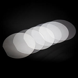
Sapphire Wafer
Manufacturing Process for High-Precision Sapphire Wafers
Crystal Material Selection
The manufacturing process begins with the selection of appropriate single-crystal sapphire material. Crystal quality, orientation, internal consistency, and dimensional availability all affect the performance of the finished wafer. Material selection must be matched with the customer’s application, including optical requirements, electrical isolation needs, thermal conditions, and downstream process compatibility.
The supplied information identifies material options associated with Corning, Nikon, Heraeus, and other sources. Because material naming and sourcing requirements can vary between projects, customers should confirm the desired material grade, crystal orientation, and certification requirements during the quotation and technical review stage.
Orientation and Cutting
After material selection, the crystal is oriented and divided into wafer blanks. Orientation is important because the physical and processing behavior of a crystal can vary according to its crystallographic plane. The selected orientation should correspond to the requirements of the intended semiconductor, optoelectronic, or optical application.
Precision cutting is performed to create wafer blanks with controlled diameter and thickness allowance. Cutting must minimize subsurface damage and maintain sufficient material uniformity for later grinding and polishing. The quality of this initial stage influences material utilization, processing time, edge integrity, and final yield.
Grinding and Thickness Control
Grinding removes cutting damage and brings the wafer closer to its specified thickness. It also helps establish parallelism and prepare both surfaces for fine polishing. Since sapphire is extremely hard, this stage requires carefully selected abrasives, stable process parameters, and controlled equipment conditions.
Thickness control is essential for consistent handling and device fabrication. The standard configurations include thickness values of approximately 500 micrometers for four-inch wafers, 625 micrometers for five-inch wafers, 675 micrometers for six-inch wafers, 725 micrometers for eight-inch wafers, and 900 micrometers for twelve-inch wafers. Customized thicknesses are also available.
Lapping and Polishing
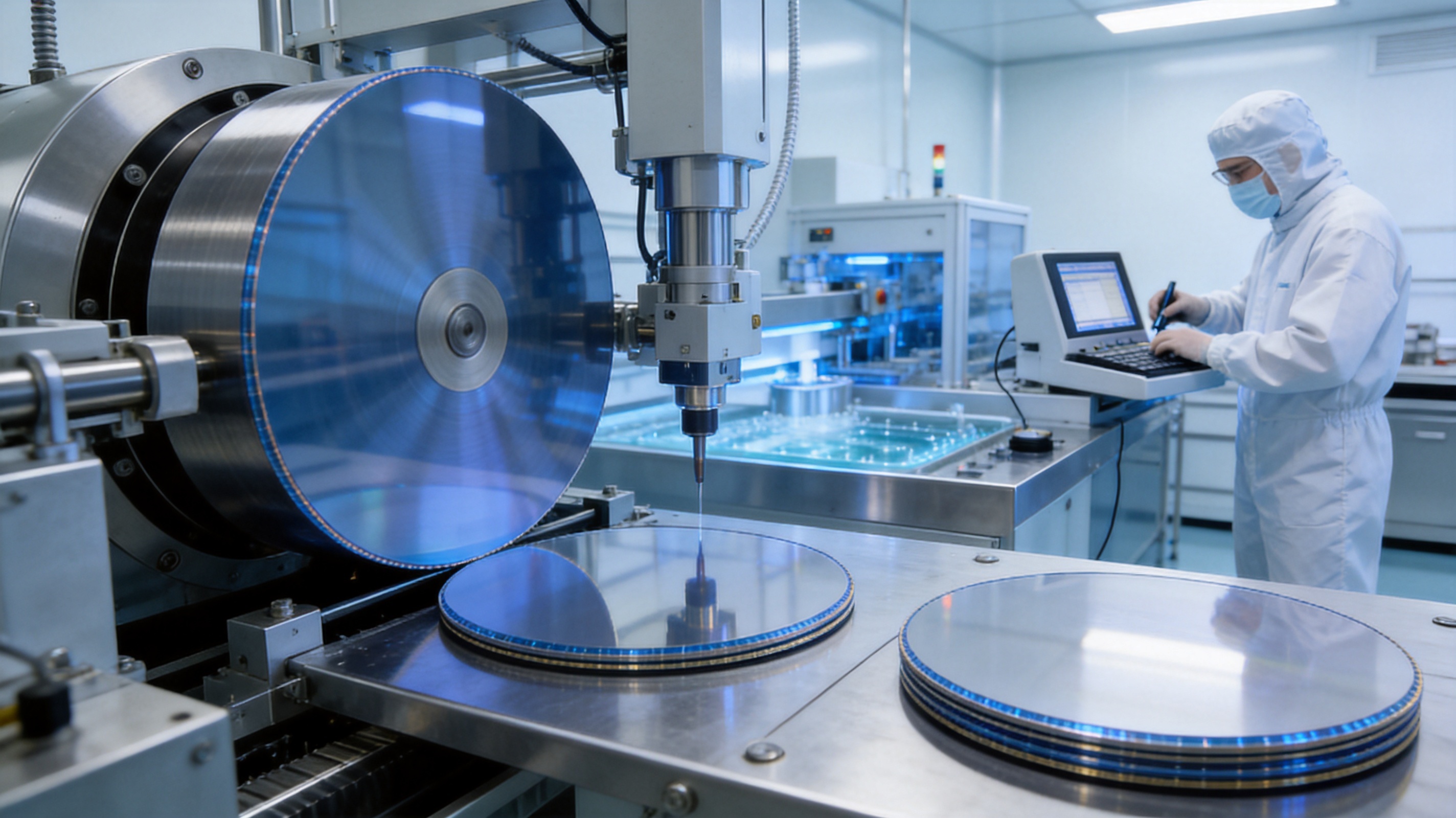
Lapping and polishing refine the wafer surfaces and remove the microscopic damage created during earlier material-removal stages. The objective is to achieve the required roughness, flatness, surface quality, and optical condition while preserving the dimensional geometry of the wafer.
Polishing sapphire requires careful balance. Excessive removal may reduce thickness uniformity or alter flatness, while insufficient removal may leave scratches, pits, or subsurface damage. A controlled polishing process therefore contributes directly to the stated Ra ≤ 1 nanometer roughness and 20/10 surface quality targets.
Edge Inversion and Shaping
After the main wafer surfaces have been processed, the edge may be shaped according to the selected configuration. A 45-degree inverted edge, SEMI-type edge, or C-shaped profile can be used depending on equipment compatibility and customer preference.
Edge shaping must be performed without introducing cracks or excessive residual stress. The finished edge should be smooth, consistent, and resistant to chipping during handling. Since edge defects can become sources of particles or wafer breakage, edge inspection is an important part of the quality process.
Cleaning and Surface Preparation
Precision cleaning removes polishing residues, particles, and other contaminants from the wafer surfaces. Cleanliness is essential for semiconductor and optoelectronic applications because even small particles can interfere with film deposition, bonding, lithography, coating, or electrical testing.
Cleaning methods must be compatible with the wafer material and the customer’s packaging requirements. Depending on the application, wafers may be supplied in a condition suitable for further customer processing, or additional cleaning and packaging specifications may be defined during technical discussions.
Inspection and Measurement
Inspection verifies whether the wafer meets the specified dimensional, surface, and visual requirements. Typical control items include diameter, thickness, thickness variation, flatness, warpage, roughness, edge profile, surface defects, and cleanliness.
The company’s experience in precision optical components supports the use of structured quality control throughout production. Its ISO9001:2015 quality management certification provides a framework for controlled processes, documentation, traceability, corrective action, and continual improvement. For automotive-related work, IATF16949 certification reflects additional experience with quality requirements associated with the automotive industry.
Environmental management is supported by ISO14001:2015 certification. Responsible environmental management is increasingly important to customers evaluating long-term suppliers, particularly in industries where material processing, water use, chemical handling, and waste reduction must be carefully controlled.
Why Precision Manufacturing Matters
Sapphire’s intrinsic properties create the potential for high performance, but they do not guarantee that every wafer will be suitable for a demanding application. A poorly finished wafer may contain excessive scratches, unacceptable curvature, uneven thickness, edge damage, or contamination. Precision manufacturing converts the advantages of the raw material into a dependable industrial product.
For semiconductor and optoelectronic customers, consistency is often as important as an individual wafer’s peak specification. A reliable supplier must produce wafers with repeatable geometry and stable surface characteristics from batch to batch. Consistency allows customers to establish process recipes, reduce adjustments, and improve production yield.
Controlled flatness and warpage also help reduce equipment-related problems. A wafer that remains stable during loading and processing is less likely to experience alignment errors, vacuum instability, or uneven contact. Controlled surface roughness improves the predictability of subsequent coatings and deposited layers.
Reliable edge quality reduces the possibility of breakage and particle generation. This is especially important when wafers are processed by automated systems. An edge profile that is compatible with standard handling equipment can support smoother integration into existing production lines.
Advantages Over Alternative Substrate Materials
Compared with Conventional Glass
Glass can provide transparency and relatively low cost, but sapphire offers substantially higher hardness, better abrasion resistance, and stronger resistance to mechanical damage. In applications involving repeated handling, particles, contact, or harsh environments, sapphire can provide longer-lasting surface integrity.
Sapphire also offers stronger performance in high-temperature and chemically demanding environments. While glass may be appropriate for many general optical uses, sapphire becomes attractive when the substrate must combine transparency with exceptional durability and electrical insulation.
Compared with Polymer Substrates
Polymers are lightweight and can be shaped economically, but they may be more vulnerable to scratching, thermal deformation, chemical attack, and long-term environmental aging. Sapphire provides a harder and more dimensionally stable alternative for precision applications.
When optical clarity must be maintained over a long operating period, the scratch resistance and thermal stability of sapphire can provide a significant advantage. Its electrical insulation and chemical durability further extend its usefulness in specialized electronic and sensor systems.
Compared with Conductive Semiconductor Substrates
Conductive substrates can be useful in many semiconductor designs, but they may not provide the electrical isolation required by every device architecture. Sapphire’s insulating behavior makes it a strong choice for applications where current must be blocked between the active device and the supporting substrate.
This isolation can support device designs with reduced parasitic interaction and improved separation between electrical elements. The best substrate depends on the full process and device structure, but sapphire provides a distinctive combination of insulation, mechanical strength, optical transparency, and thermal stability.
Compared with Lower-Grade Ceramic Materials
Many ceramics offer good heat resistance and mechanical stability, but not all provide the same optical transparency, surface finish capability, or defect control as single-crystal sapphire. Polycrystalline materials may contain grain boundaries that influence optical or mechanical behavior, whereas single-crystal sapphire provides a continuous crystal structure.
For applications requiring a transparent, hard, electrically insulating, and highly polished surface, sapphire can provide a more complete performance solution than conventional opaque ceramics.
Application Areas
Semiconductor Optoelectronics
Sapphire wafers are widely associated with semiconductor optoelectronic device manufacturing. Their electrical insulation and thermal stability provide a useful platform for the formation of active layers and device structures. The stable surface and precise geometry help support repeatable processing.
White and Blue LED Production
Sapphire is an important substrate material for the production of white and blue light-emitting diode technologies. The substrate must provide mechanical stability during epitaxial growth and subsequent device processing. Its optical and thermal characteristics also contribute to the overall suitability of the device platform.
Laser and Photonic Devices
Laser optics and photonic systems often require materials with excellent surface quality, optical transparency, dimensional stability, and resistance to environmental damage. Sapphire wafers can be used as substrates or precision optical elements in selected laser and photonic applications.
Electronic Isolation Components
Because sapphire blocks current flow, it can be used where electrical isolation between devices, sensors, electrodes, or other components is necessary. This includes specialized electronic assemblies and structures that require a nonconductive but mechanically robust base.
Sensor and Analytical Equipment
Sapphire’s transparency, chemical resistance, hardness, and thermal stability make it suitable for selected sensor and analytical equipment. In harsh measurement environments, a sapphire substrate or window can protect sensitive components while maintaining optical access.
Automotive and Industrial Optics
Automotive and industrial systems may expose optical components to vibration, particles, temperature changes, moisture, and contact wear. The durability of sapphire can be valuable in applications where surface damage would reduce optical performance or shorten product life.
Medical and Laboratory Equipment
The combination of biocompatibility, chemical resistance, electrical insulation, and cleanable surfaces allows sapphire to be considered for specialized medical and laboratory applications. Suitability depends on the complete product design, regulatory requirements, and sterilization conditions.
Customization Options
Standard products are available in four-inch, five-inch, six-inch, eight-inch, and twelve-inch diameters. The company also provides customized services for other sizes and specifications. Customization can be considered for diameter, thickness, edge design, locating feature, surface finish, flatness, roughness, and packaging.
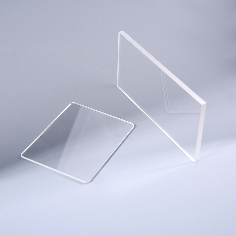
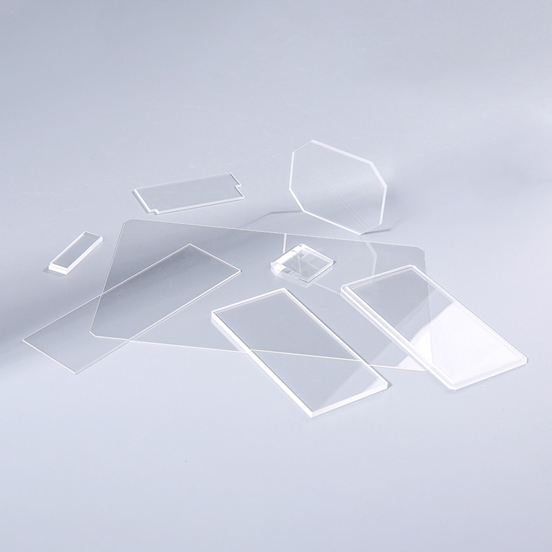
Customers requiring wafers smaller than standard diameters or special geometric formats can discuss the intended dimensions during the inquiry stage. Customized products may be suitable for research institutions, prototype development, special semiconductor processes, and equipment-specific applications.
Customization is most effective when the customer provides complete technical information. Important details include the required diameter, thickness, crystal orientation, surface condition, flatness, warpage, roughness, surface quality, edge configuration, quantity, inspection requirements, and packaging method.
For development projects, it is also useful to provide information about the downstream process. Deposition temperature, bonding method, coating type, cleaning chemistry, equipment model, and handling method can influence the recommended wafer design. Technical communication at the beginning of a project helps reduce unnecessary revisions and supports a more efficient transition to production.
Company Manufacturing Strengths
Changzhou Haolilai Photo-Electricity Scientific and Technical Co., Ltd. was founded in 1998 and is located in Changzhou, Jiangsu, China. The company occupies approximately 35,000 square meters and has more than 300 employees. Its activities are focused on precision optical components and related products for laser optics, automotive optics, semiconductor optics, and consumer optics.
The company’s long operating history provides experience in precision processing and industrial customer service. Its technical team supports product development, process improvement, customization, and quality control. The company has established the Jiangsu Precision Optical Lens Engineering Technology Center and the Jiangsu Enterprise Technology Research Center, supporting continued research and technical development.
HLL has obtained ISO9001:2015, ISO14001:2015, and IATF16949 certifications. These certifications support a structured approach to quality management, environmental management, and automotive-industry quality requirements. The company has also received recognition as a High-Tech enterprise in Jiangsu Province.
Its intellectual property portfolio includes invention patents, utility model patents, and Jiangsu High and New Tech Products. More than 30 certificates and patents support the company’s technical profile and demonstrate continued investment in product development.
The company exports to more than 20 countries. International experience is valuable because overseas customers often require clear specifications, stable packaging, traceable quality documentation, and consistent communication throughout the order process.
The combination of technical personnel, manufacturing resources, quality systems, research centers, and industry experience provides a foundation for producing sapphire wafers according to demanding specifications. Customers benefit from access to both standard products and customized manufacturing support.
Quality Management and Customer Support
Quality control begins with reviewing the customer’s technical requirements and continues through material selection, processing, inspection, and packaging. A controlled workflow helps ensure that the finished wafer is evaluated against the same criteria used during quotation and production planning.
For high-precision wafers, documentation can be as important as the physical product. Customers may require dimensional inspection results, surface quality records, material information, batch identification, or certificates of conformity. These requirements should be discussed before production so that the appropriate inspection and documentation plan can be established.
Packaging must protect the wafer against scratches, particles, moisture, and mechanical impact during storage and transportation. The correct packaging method depends on the wafer diameter, surface finish, quantity, and cleanliness requirement. Customers can specify packaging expectations as part of the order review.
Technical support is also important when a customer is selecting between standard and customized specifications. A wafer that is unnecessarily thick may increase material and processing costs, while a wafer that is too thin may not provide sufficient mechanical stability. Similarly, an overly demanding surface specification may increase processing time without delivering practical value for the intended application.
By reviewing the complete use case, the supplier and customer can select an appropriate balance of performance, reliability, and cost. This approach is particularly beneficial for new products and applications in which the wafer specification has not yet been fully standardized.
How to Select the Right Sapphire Wafer
Define the Required Diameter
The wafer diameter should match the customer’s equipment, mask size, handling system, and production plan. Standard options include four-inch, five-inch, six-inch, eight-inch, and twelve-inch wafers. If the equipment uses a different dimension, a customized diameter may be considered.
Confirm Thickness and Tolerance
Thickness affects mechanical strength, weight, thermal behavior, and compatibility with handling tools. Customers should specify the nominal thickness and acceptable tolerance. If the wafer will undergo additional thinning, bonding, or polishing, the starting thickness should be selected accordingly.
Specify Surface Requirements
Surface roughness, flatness, warpage, scratch and dig limits, and cleaning condition should be defined based on the downstream process. A deposition process, optical application, and bonding application may require different surface characteristics.
Select the Edge Configuration
The edge should be compatible with the customer’s equipment and handling method. Options include a 45-degree inverted edge, SEMI-type edge, or C-shaped edge. Locating edges and locating angles should also be specified when orientation control is required.
Identify Material and Orientation Needs
Material source, crystal orientation, and any required documentation should be confirmed before production. The correct orientation can be important for epitaxial growth, optical behavior, thermal characteristics, or device performance.
Review Quantity and Delivery Requirements
Prototype quantities, sample orders, pilot batches, and mass-production requirements may require different planning approaches. Customers should provide an estimated annual demand or project schedule when possible so that production capacity and delivery planning can be evaluated.
Frequently Asked Questions
What is the main advantage of a sapphire wafer?
The main advantage is the combination of high hardness, electrical insulation, optical transparency, chemical resistance, thermal stability, and mechanical durability. This combination makes sapphire suitable for demanding semiconductor, optoelectronic, optical, and industrial applications.
What standard wafer diameters are available?
Standard products are available in four-inch, five-inch, six-inch, eight-inch, and twelve-inch diameters. Other sizes can be discussed as customized products.
What thicknesses are available?
The listed typical thicknesses are 500 ± 5 micrometers for four-inch wafers, 625 ± 5 micrometers for five-inch wafers, 675 ± 5 micrometers for six-inch wafers, 725 ± 5 micrometers for eight-inch wafers, and 900 ± 5 micrometers for twelve-inch wafers. Customized thicknesses are available according to application requirements.
Can the wafers be supplied with special edges?
Yes. Available edge configurations include a 45-degree inverted edge, SEMI-type edge, and C-shaped edge. The preferred configuration should be selected according to the customer’s equipment and handling process.
What are the stated flatness and warpage specifications?
The stated flatness specification is no more than three micrometers, and the stated warpage specification is no more than ten micrometers for the listed wafer sizes.
What surface roughness can be achieved?
The listed specification is Ra ≤ 1 nanometer. The final roughness requirement should be confirmed according to the intended application and inspection method.
Are sapphire wafers electrically conductive?
Sapphire is an electrical insulator and effectively blocks current flow. This makes it suitable for applications requiring electrical isolation between devices and components.
Are sapphire wafers suitable for LED applications?
Yes. Sapphire is widely used as a substrate material for semiconductor optoelectronic devices, including white and blue LED-related applications.
Can sapphire wafers be used in high-temperature environments?
Sapphire provides strong high-temperature resistance and is suitable for many elevated-temperature processing and operating environments. The exact temperature limit should be evaluated according to the complete application and process conditions.
How does sapphire compare with ordinary glass?
Sapphire is harder, more scratch-resistant, and generally more durable than ordinary glass. It also offers strong chemical and high-temperature resistance while maintaining optical transparency and electrical insulation.
Can the company provide customized wafers?
Yes. Customized services can be considered for diameter, thickness, surface finish, flatness, warpage, edge design, locating features, and other technical requirements.
What information should be included in an inquiry?
An inquiry should include diameter, thickness, tolerance, crystal orientation, surface roughness, flatness, warpage, surface quality, edge configuration, quantity, packaging requirements, and intended application. Information about downstream processing is also helpful.
What industries does the manufacturer serve?
The company serves customers in laser optics, automotive optics, semiconductor optics, consumer optics, optoelectronics, and related precision manufacturing fields.
What quality certifications does the company hold?
The company has obtained ISO9001:2015, ISO14001:2015, and IATF16949 certifications. It is also recognized as a High-Tech enterprise in Jiangsu Province.
How can customers request more information?
Customers can contact the sales team of Changzhou Haolilai Photo-Electricity Scientific and Technical Co., Ltd. for product specifications, customization feasibility, quotations, samples, technical documents, and delivery information.
Conclusion
High-precision sapphire wafers provide a strong foundation for semiconductor, optoelectronic, optical, electronic, automotive, laboratory, and industrial applications. Their combination of hardness, scratch resistance, electrical insulation, transparency, thermal stability, chemical resistance, impact resistance, and biocompatibility gives them clear advantages over many conventional substrate materials.
However, the value of sapphire depends on precision processing. Controlled diameter, thickness, roughness, flatness, warpage, surface quality, edge geometry, cleanliness, and inspection are necessary to transform a high-performance crystal into a reliable industrial wafer. The listed specifications, including Ra ≤ 1 nanometer roughness, flatness of no more than three micrometers, warpage of no more than ten micrometers, and 20/10 surface quality, demonstrate the level of control required for demanding applications.
Changzhou Haolilai Photo-Electricity Scientific and Technical Co., Ltd. combines experience in precision optical manufacturing with quality certifications, technical research capabilities, customized production, and international service. Its sapphire wafer products are available in standard four-inch through twelve-inch formats, with additional sizes and specifications available by request.
For customers seeking a durable, electrically insulating, optically transparent, and highly stable substrate, sapphire wafers offer a dependable solution. Careful specification review and cooperation with an experienced precision manufacturer can help ensure that the selected wafer meets both current process requirements and long-term product performance objectives.
References
1. Changzhou Haolilai Photo-Electricity Scientific and Technical Co., Ltd., Sapphire Wafer Product Information and Technical Specifications.
2. Changzhou Haolilai Photo-Electricity Scientific and Technical Co., Ltd., Corporate Technical and Certification Information.
3. International Organization for Standardization, Quality Management Systems — ISO 9001:2015.
4. International Organization for Standardization, Environmental Management Systems — ISO 14001:2015.
5. International Automotive Task Force, Automotive Quality Management System Standard — IATF 16949.
6. Semiconductor Equipment and Materials International, General Semiconductor Wafer and Edge Profile Practices.
7. Optical Society and Precision Optics Industry References, Scratch and Dig Surface Quality Classification.


 苏公网安备32041102000130号